Homework_2: Custom Cell Layout
Revised 08 Oct. 2010 by D. Bouldin
HW2 can now be executed on ada7, ada8 or ada9.
ECE 651 homework will NOT be fabricated but will use rules and standard cells for an open
50nm (FreePDK45nm) process:
Spice Models
SPICE Command Summary
Standard Cells Spice Netlists (trans. sizes)
Standard Cells (LEF)
Standard Cells (sizes)
FreePDK Design Rules
Standard Cells (Data Sheets)
Standard Cells (400nm Schematics/Layouts)
651-std-cells (8 Oct)
Simulation Tips
Note: The grid layer is "hilite d3" (LSW-->Edit-->Set Valid Layers).
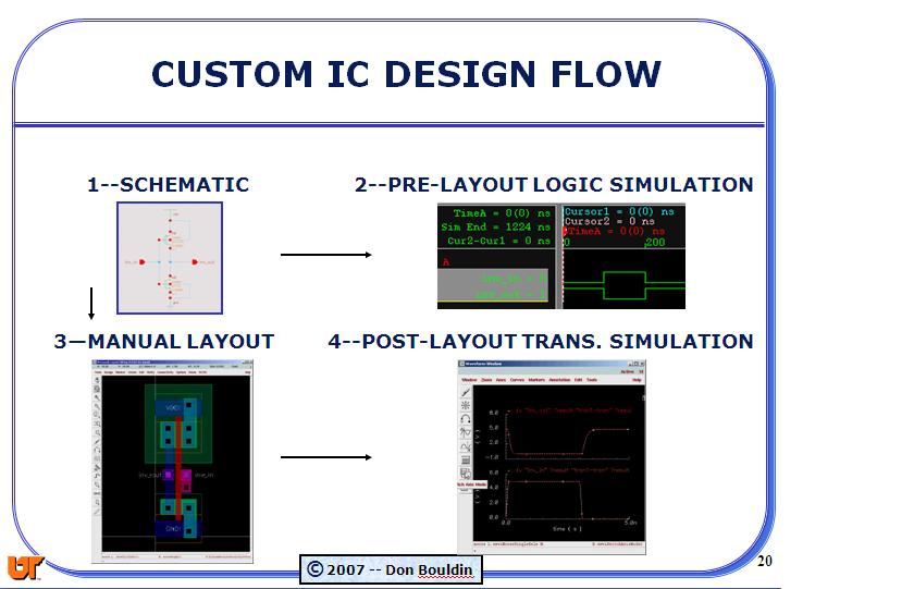
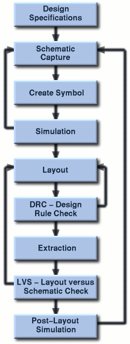
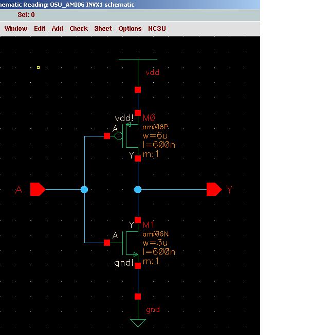
HW2a: Follow the Schematic Capture Tutorial to generate:

HW2b: Add a testbench around your inverter schematic:

Select Create-Instance and in the Component Browser window,
select analogLib-->Passives-->Cap
and fill in the dialog box
Select analogLib-->Globals--->Vdd and gnd
Select analogLib-->Sources--->Independent-->Vdc and vpulse
and fill in the Vdc dialog box
and fill in the vpulse dialog box
HW2c: Follow the Hspice Tutorial to perform pre-layout simulation using ADE-XL and Hspice.
input.ckt
pre-layout waveform
HW2d: Follow the Layout Tutorial to generate a layout (with rulers).
To save time, you may copy and edit the OSU layout until it looks like this (with pfet W=750):
Layout
HW2e: Follow the LVS, DRC & Extraction Tutorial to perform LVS, DRC and Extraction.
HW2f: Perform post-layout simulation to verify your design.
PEX instructions
input.ckt_post
INVX1.pex.netlist.INVX1.pxi
post-layout waveform
Link your results to your web home page and update hw.html
************** Old Homework 2 ****************
FreePDK Design Flow
OSU Hspice Tutorial
NCSU Analog Artist with Hspice Tutorial
Our files are located on ada10 under: /sw/cadence/FreePDK45-1.3/osu_soc/lib/
Nangate Open 45-nm Standard Cells
PART A: Follow this TUTORIAL to implement your own version of OSU-INVX1.
Include rulers in your layout.
Post your own results for schematic, pre-layout simulation, layout, DRC check
and post-layout simulation as gif/jpg files on your protected webpage.
ECE 491 Tutorial
PART B: Repeat the tutorial by copying and editing the schematic and layout for OSU-NANDX1.
Make the pfets 7.5-micron or 25-lambda wide. Post your own results.
Include rulers in your layout.
ECE 433 projects are fabricated via MOSIS by ON Semiconductor (formerly AMI)
on its 600nm process using a conservative feature size of 0.6-micron and a lambda of 0.3.
The SCMOS_SUBME (with second poly or electrode layer, "elec")
rules
are used with the following layer map. Note 600nm Spice models and results from MOSIS.
600nm Standard Cells (LEF)
400nm Standard Cell Library (schematics, etc.)
MOSIS fab schedule

OSU-inverter with ruler (pdf)
DFFPOSX1
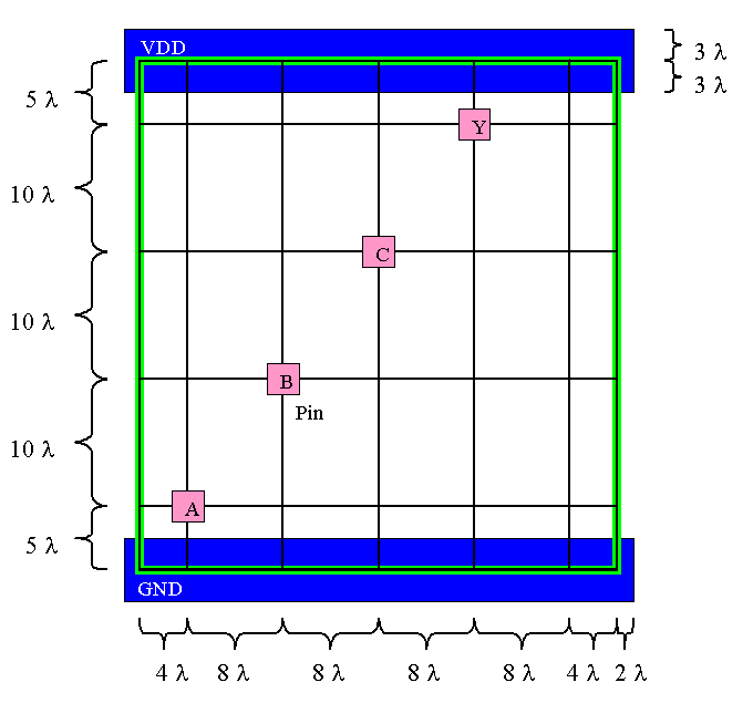
Simple Rules            lambda
----------------------- ------
1. min. width of active = 10
2. min. width of poly   =  2
3. min. poly extension  =  2
4. min. wire separation =  4
5. min. width of metal  =  4
6. contacts are 4x4

Note: active surrounded by n-select --> ndiff
      active surrounded by p-select --> pdiff
Hints for Part B:
Copy an existing (read-only) standard cell (schematic or layout) into your own library.
Use "Add Instance" and access "OSU_AMI06 --> NANDX1 --> schematic".
Use "Create Instance" and access "OSU_AMI06 --> NANDX1 --> layout".
Select the symbol and then select "Edit --> hierarchy flatten".
Edit the schematic and layout as needed.
Remove any existing pins and create new ones; otherwise, LVS may trigger a mismatch.
When you click on "create ---> pins" a box will pop-up for you to supply "pin-name".
At the bottom, select "Access direction" and disable everything except "Left and Right"
for VDD and GND and "Top and Bottom" for inputs and outputs.
Wiring can be facilitated using "Create Path".
Metal-2 rules dictate the horizontal spacing of 1.6u or 8-lambda
while Metal-3 rules dictate the vertical spacing of 2.0u or 10-lambda.
Using a grid permits the cell boundaries to overlap horizontally by 4.8u (16-lambda).
Note: The grid layer is "hilite d3" (LSW-->Edit-->Set Valid Layers).
It is best to place pins (4x4 contacts) at a grid intersection.
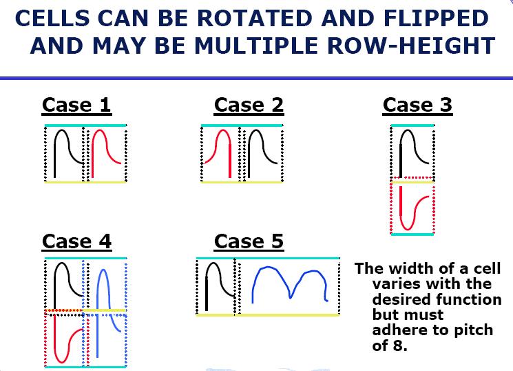
Case 2:
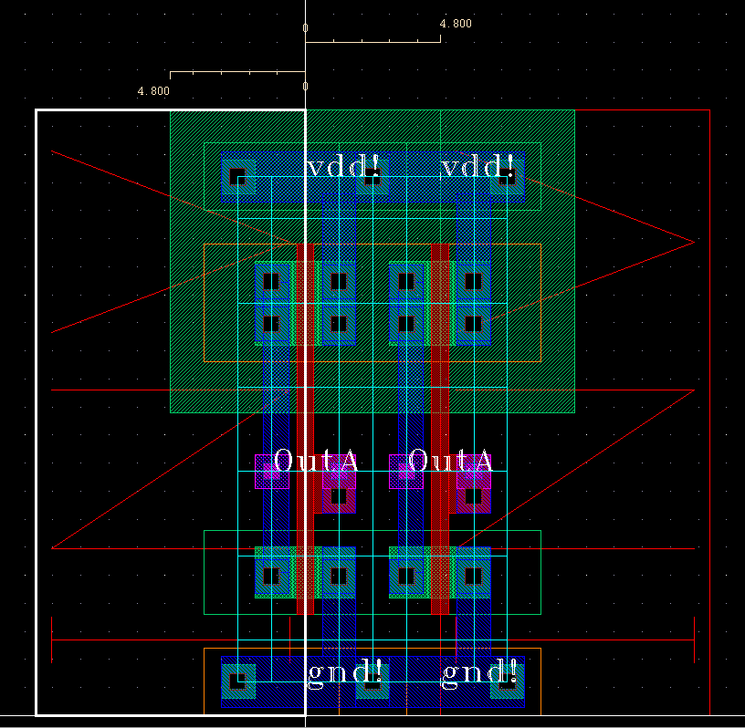
The vertical overlap of the cell boundaries is 4.8u (vdd) or 2.4u (gnd):
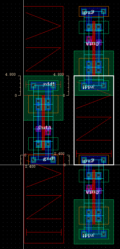
Note how the individual cell grids overlap horizontally by (4-lambda)
and vertically by (5-lambda):
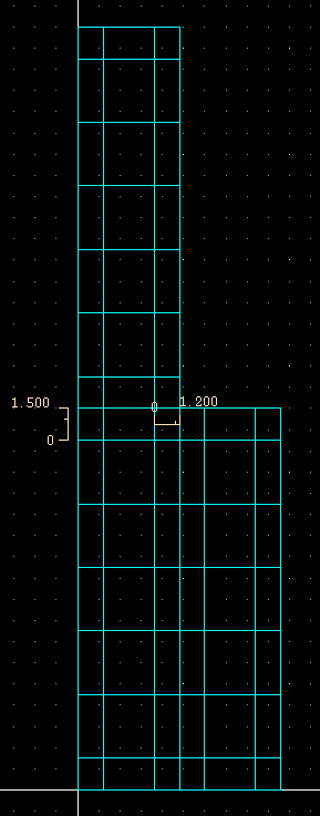
Standard-Height Cell Grid:
OSU Grid
Spectre Circuit Simulator User Guide (334 pages -- pdf)
Link your results to your restricted webpage.
Update hw.html
dbouldin@tennessee.edu