Homework_4 -- Loading Effects and Sizing Transistors

D-FlipFlop
Determining the Clock Period
Note the latest Spice & RC measurements for AMI06.
Sheet Resistance
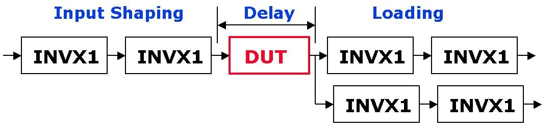
Using the INVX1 and FAX1 from the OSU_FreePDK library,
construct a 4-bit adder (as the DUT) and add shaping inputs and loads.
Connect two INVX1 cells in series to shape the Carry-in of the LSB slice.
Connect two INVX1 cells in series to the MSB-Sum. Repeat this for the MSB-Carry-Out.
All of the A inputs of the 4-bit adder should be connected to Vdd and
all of the B inputs of the 4-bit adder should be connected to GND.
The other three sets of outputs of the 4-bit adder should be left unconnected.
Thus, the schematic with no load will look like this
The schematic with 4 loads will look like this
Simulate pre-layout using HSPICE,
and then draw a single-row layout.
Make connections between cells with metal-1 or metal-2.
Perform drc, extraction, lvs and simulate post-layout using HSPICE.
Be sure to extract parasitic capacitance for the post-layout simulations.
For the HSPICE simulation, apply the following to the input of the shaping INVX1 chain of the LSB Carry-in input:
Vin (Cin 0) vsource type=pwl wave=[0n 0 3n 0 3.5n 0.5 4n 1.1 10n 1.1]
tran1 tran start=0 stop=10n step=0.05n errpreset=moderate
Do not add any capacitors on any output nodes since the INVX1 cells add just what is needed.
Measure the delay for each case (except case-7) from the mid-point of the LSB Carry-in adder input
to the mid-point of the MSB Carry-out adder output.
Record only the delay from a rising Cin to a change in MSB Carry-out for each case.
Note my OLD pre-layout spectre results for noload show a delay
of 2.2 ns from a rising Cin-adder4
at the 2.5 volt level to a rising Cout at the same level.
For case-7, measure the delay from the mid-point of the LSB Carry-in adder input
to the mid-point of the BUFX4-output.
Make a table of your post-layout delays and plot Delay vs. #loads.
CASE:
(1) 4-bit adder with no load
(2) 4-bit adder with 1 load-chain
(3) 4-bit adder with 4 load-chains
(4) 4-bit adder with 8 load-chains
(5) 4-bit adder with 1 load-chain interconnected with 1000-micron metal-1 wire (1.2-microns wide)
(6) 4-bit adder with 1 load interconnected with 1000-micron poly wire (1.2-microns wide)
(7) 4-bit adder followed by BUFX4 with 8 load-chains
(8) 4-bit adder with larger internal W's in the MSB-slice to achieve the same delay as case 7.
(Just copy case 4 to be case 8 and edit the W's to have the same delay as case 7.)
Discuss your results for each case. Note that case-5 should be slower than case-2 and case-6
should be even slower.
MOSIS Process Monitor & Testing
Scaling
350 nm
250 nm
180 nm
AMI06 Library (protected html)
TSMC018 Library (protected html)
AMI06 Delay (protected jpg)
TSMC018 Delay (protected jpg)
OSU_45 Library (protected html)
Library Characterization (html)
IBM 180nm Library Databook (pdf)
Link your results to your web home page.
Update hw.html
dbouldin@tennessee.edu