Very Helpful Tips
Part A -- Delay Measurements
NanoSim is a fast Spice simulator which uses the same format as Hspice.
Login to ada3.eecs.utk.edu
Open your schematic from hw4-case-1:
---- 2010: You already have the HSPICE file so you can skip this next section.
Click on Tools --> Analog Environment
Select the Hspice simulator:
Click on Setup --> Simulator/Directory/Host and select hspiceS
Generate the netlist:
Click Simulation --> Netlist --> Create Final
Change directory to "simulation/adder4-noload/hspiceS/schematic/netlist"
Copy "hspiceFinal" to "adder4-noload.spi"
Edit "adder4-noload.spi" to include:
./usr/local/ncsu/ncsu-cdk-1.5.1/models/hspice/standalone/ami06N.m
./usr/local/ncsu/ncsu-cdk-1.5.1/models/hspice/standalone/ami06P.m
--------- 2010: Skip to here and use 1.1 volts instead of 5 volts.
vCIN CIN 0 pwl(0n 0 3n 0 3.5n 2.5 4n 5 10n 5)
.tran 0 10n 0.05n
Vdd vdd! 0 dc=5
vgnd gnd! 0 dc=0
(My edited adder4-noload.spi (using AMI06) is included in the tar file in Part B below.)
Create a NanoSim configuration file named "nanosim.cfg" with the following contents:
print_node_voltage *
print_node_logic *
Then, type:
export SNPSLMD_LICENSE_FILE="27011@synopsys-lic.eecs.utk.edu"
nanosim -n adder4-noload.spi -c nanosim.cfg -out fsdb
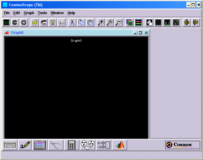
Synopsys CosmosScope can be used to view the waveforms produced by NanoSim.
Type:
cscope &
The following window will open:
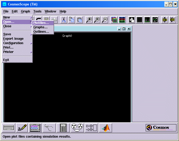
 Next, select File --> Open --> Plotfiles
and choose nanosim.fsdb
Next, select File --> Open --> Plotfiles
and choose nanosim.fsdb
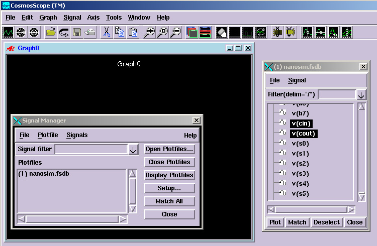
 Next, open your file and select the relevant signals to display:
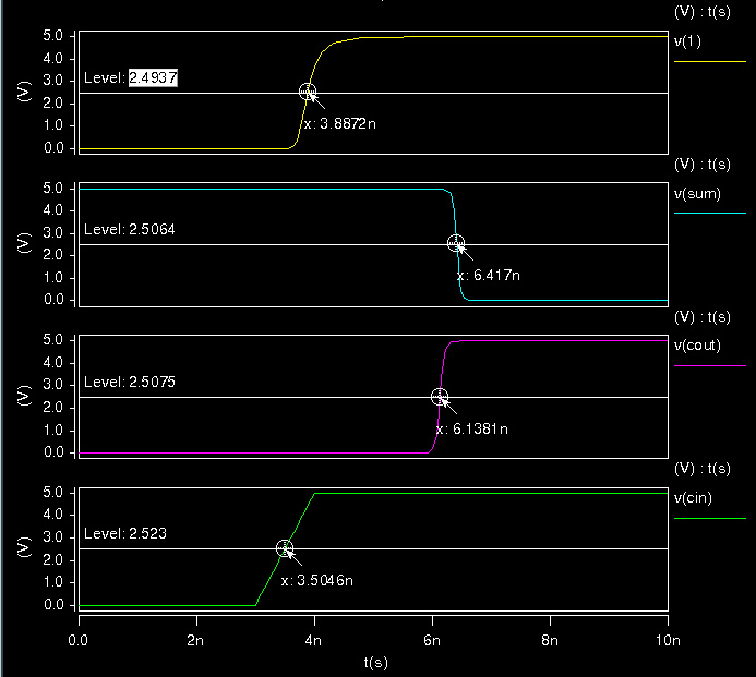
 Measure the delay from carry_in to carry_out by clicking the "At Y Measurement" icon
and then select "Signal --> Measure Results" and capture the image.
In the graph below, v(1) is the carry_in of the adder while v(cin)
is the input to the first inverter.
Measure the delay from carry_in to carry_out by clicking the "At Y Measurement" icon
and then select "Signal --> Measure Results" and capture the image.
In the graph below, v(1) is the carry_in of the adder while v(cin)
is the input to the first inverter.
Part B -- Power Measurements
Using the same methodology as in Part A, we will now explore the power measurement
capabilities of NanoSim.
This tutorial was adapted from one provided by Synopsys in two formats: pdf and swf.
A similar tutorial is available at chiptalk.org.
cp ~bouldin/webhome/protected/651-hw10/651-hw10.tar .
tar -xvf 651-hw10.tar
cd 651-hw10
The file "setup.spi" contains an adder circuit and "adder.vec"
contains a series of digital input vectors to stimulate the circuit.
This is called the "switching activity".
The "run" file contains:
nanosim -n setup.spi -nvec adder.vec -C cfg
Now, type:
export SNPSLMD_LICENSE_FILE="27011@synopsys-lic.eecs.utk.edu"
./run
Note that two errors have been captured in the "nanosim.err" file
which can be viewed by typing:
viewerror -i nanosim.err -o errors
and then:
vi errors
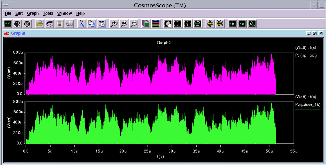
The power report is given in "nanosim.log".
(Also, see power.swf.)
To view the power report in a graphical format, type:
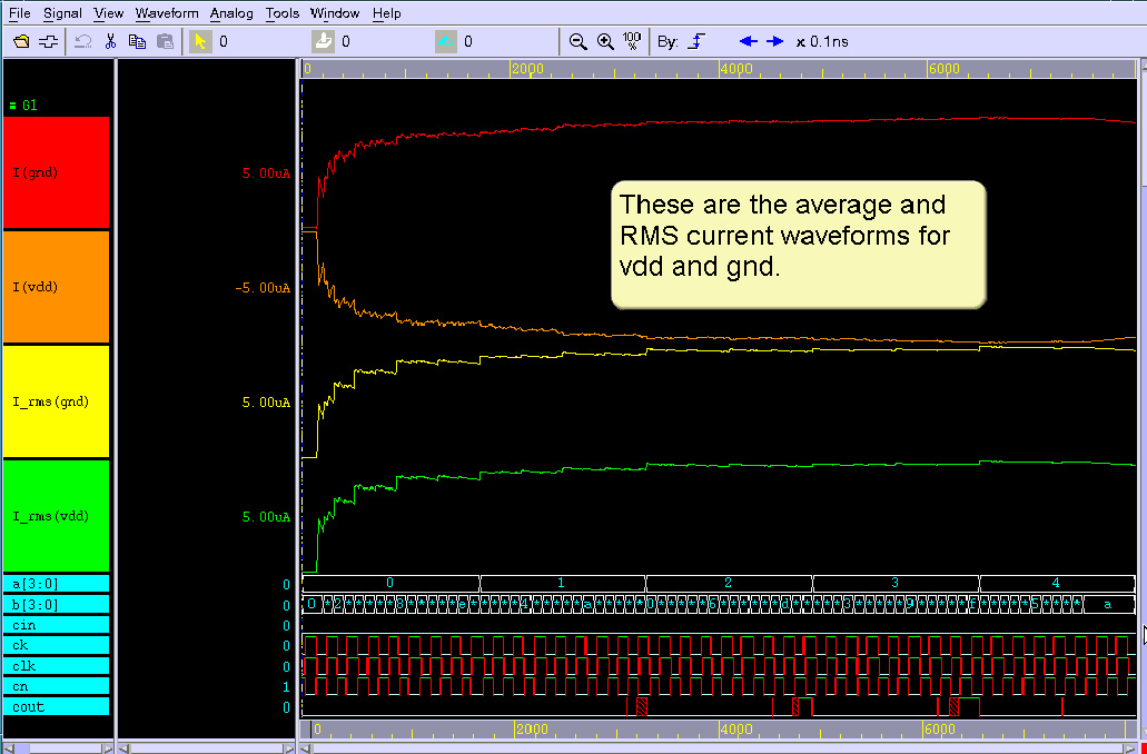
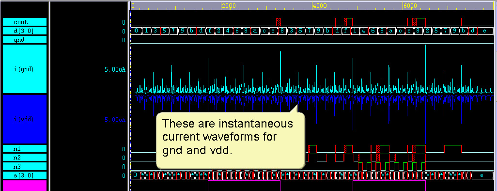
Use cscope to view the results which will be like the ones shown below (using nwave).
Part C -- Power Measurements on Your Circuit
Adapt the files in Part B to determine the power of your
homework_4 circuits for adder4-noload and adder4-4loads.
Match the labels in your spi files to those in adder.vec
The homework_4 circuits had their a[0-3] and b[0-3] inputs
tied to Vdd and Gnd. Change the node labels in the spi
file to make these variable.
Replace: XI0 VDD! 0 NET52 COUT SUM FAX1_G2
with: XI0 a[3] b[3] NET52 COUT SUM FAX1_G2
Also, remove: vCIN CIN 0 pwl(0n 0 3n 0 3.5n 2.5 4n 5 10n 5)
Make other changes in your spi files as needed to match the labels in adder.vec
Post your results on your protected webpage.
===========
Note that power estimates can be made at multiple levels
as described in the thesis (PDF and PPT) by Ashwin Balakrishnan.
 NanoSim can also be used to simulate a mixture of analog and digital circuits
for full-chip mixed-signal simulation: NS-VCS-MX.pdf
NanoSim can also be used to simulate a mixture of analog and digital circuits
for full-chip mixed-signal simulation: NS-VCS-MX.pdf
