Homework_2: Custom Cell Layout
Revised 01 September 2011 by D. Bouldin
HW2 can now be executed on ada8 and ada9.
ECE 651 homework will NOT be fabricated but will use rules and standard cells for an open
50nm (FreePDK45nm) process:
Spice Models
SPICE Command Summary
Standard Cells Spice Netlists (trans. sizes)
Standard Cells (LEF)
Standard Cells (sizes)
FreePDK Design Rules
Standard Cells (Data Sheets)
Standard Cells (400nm Schematics/Layouts)
651-std-cells
Simulation Tips
Note: The grid layer is "hilite d3" (LSW-->Edit-->Set Valid Layers).
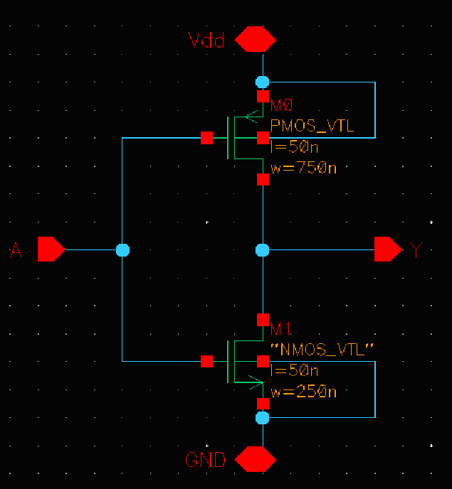
HW2a: Follow the Schematic Capture Tutorial to generate:
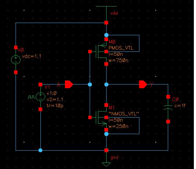
HW2b: Add a testbench around your inverter schematic:
Simulation Tips
Select Create-Instance and in the Component Browser window,
select analogLib-->Passives-->Cap
and fill in the dialog box
Select analogLib-->Globals--->Vdd and gnd
Select analogLib-->Sources--->Independent-->Vdc and vpulse
and fill in the Vdc dialog box
and fill in the vpulse dialog box
HW2c: Follow the Hspice Tutorial to perform pre-layout simulation using ADE-XL and HspiceD.
Use Cadence to invoke Hspice instead of running it in stand-alone mode so you can view the waveform.
input.ckt
pre-layout waveform
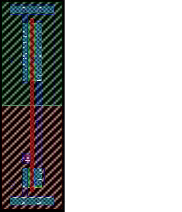
HW2d: Follow the Layout Tutorial to generate a layout (with rulers).
To save time, you may copy and edit the OSU layout until it looks like this (with pfet W=750):
HW2e: Follow the LVS, DRC & Extraction Tutorial to perform LVS, DRC and Extraction.
HW2f: Perform post-layout simulation to verify your design.
PEX instructions
PEX Hints
input.ckt_post
INVX1.pex.netlist.INVX1.pxi
post-layout waveform
Note the delay from input to output changes from pre-layout to post-layout.
(e.g. 6.8ps-->9.3ps). Comment on why.
Link your results to your web home page, describe the lessons you learned and then update
hw.html
dbouldin@tennessee.edu