Design and Implementation of
a Microelectronic System
String Comparator
Mohammad Ahsanul Adeeb & Mohammad Moshiur Rahman
ECE551 FINAL PROJECT REPORT
December 1, 2004
Electrical and
Computer Engineering
The
University of Tennessee
Knoxville,
TN 37996
Contents
- Abstract
- Introduction
- String Comparator
- Algorithm for Edit Distance
- System Requirements
- ASIC Requirements
- Block Diagrams
- Flow Charts
- Pre-Synthesis Simulation Results
- Placement and Routing Post-Synthesis Simulation Results
- Implementation in the Altera Tools
- System Performance
- Conclusion
- References
List of Figures
- Design Flow for a Microelectronic
System
- System-level Block Diagram
- ASIC Modules
and I/O requirements
- Block
Diagram of the Test Bench
- Block Diagram of the Main Module
- Block Diagram of theEdit Module
- Zooming in to the Block Diagram
of the Edit Module
- Flow Chart of the Search Module
- Zooming in to the Search Module
Flow Chart
- Test Bench Simulation
- Edit Module Simulation
- Search Module Simulation
- Floor Plan for Altera FLEX
10K20
- Layout in Xilinx XCV1000E
- Zooming in to the Virtex Layout
- Test Bench Simulation
- Edit Module Simulation
- Search Module Simulation
- Test Bench Simulation in Virtex
- Post-Synthesis Coverage for
Virtex
- Altera Logic Floorplan
Abstract
This project
involves the design, simulation, realization and demonstration of a STRING
COMPARATOR system using multiple (Altera and Xilinx) Field-Programmable Gate
Arrays (FPGA). The behavior of the system was described in a hardware
description language (VHDL), which was then synthesized into a
hardware-independent structural description and then combined with other
components. After verification of the design using computer simulation, the
design was physically placed and routed using technology-dependent tools,
namely Altera & Xilinx tools.
Introduction
The design of
the microelectronic system for this project was done to meet the requirements
for a specific application. The system consists of input/output devices coupled
with digital logic circuitry, to be implemented in a single
application-specific integrated circuit (ASIC). The design is specified, as
shown in Figure 1, at various levels of abstraction including the system,
behavioral, structural, and physical levels. The design process involves
mapping the requirements of the application into lower-level specifications
that describe not only the internal functions, but also the interactions among
the components and the external world.
For this
project, a hardware description language, VHDL, was used to specify portions of
the design. This representation was then synthesized and mapped into a chosen
technology. The resulting structural (logic) description then was combined with
other components using a schematic editor. After that the design was simulated
for functionality. Once verified, the structural representation was translated
into a physical representation that was placed and routed automatically. The
design was then re-simulated to verify proper operation and timing.
Using this
synthesis-based approach, the core of the design was made to be
technology-independent. Then it could be implemented on multiple devices;
namely the Altera FLEX10K20 and Xilinx XCV1000E devices. Very little redesign would be required for transferring the
design from one platform to another. This platform-independence facilitates
cost-effectiveness and turnaround time for real-world designs that may be
targeted to a variety of devices. In addition, various devices can be compared
on the basis of speed, cost, size, and availability while maintaining the exact
same functionality.
This report has
been organized along the lines of the design flow shown in Figure 1. First, the
system requirements and then the detailed specifications are given. Next, the
behavioral and structural representations are discussed. The actual physical
layouts were implemented after successful design synthesis and verification by
simulation for the specific technology mentioned.
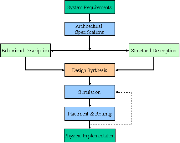
Figure 1: Design Flow for a Microelectronic System
String Comparator
A string comparator is basically a system that compares two strings and tries to measure the similarity between two based on some mathematical calculations. In many applications it is necessary to determine the similarity of two strings. A widely used notion of measuring string similarity is the Levenshtein Distance or the edit distance. The edit distance of two strings, which we refer to as the source string (s) and the target string (t), is defined as the minimum number of point mutations required changing s into t, where a point mutation is one of the following:
1. Changing a letter,
2. Inserting a letter or
3. Deleting a letter
For example,
- If s is "test" and t is "test",
then LD(s,t) = 0, because no transformations are needed. The strings are already
identical.
- If s is "test" and t is "tent",
then LD(s,t) = 1, because one substitution (change "s" to
"n") is sufficient to transform s into t.
The greater the Levenshtein distance, the more different the strings are. Levenshtein distance is named after the Russian scientist Vladimir Levenshtein, who devised the algorithm in 1965.
More Examples:
1)

Edit Distance = 0
2)

Distance
without shifting: 5 (for deleting five
characters) + 5 (for inserting five characters) = 10
Distance
after shifting: 2 (for deleting two
characters) + 2 (for inserting two characters) = 4
Edit Distance = 4
Our designed string comparator calculates the edit
distance between two strings according to the definitions described above, and
it also incorporates the additional feature of a substring search. For the
search option, a small string is looked for inside a bigger string for a
possible match. If match occurs, the system reports that as well as the
position in the bigger string where the match occurs. Detailed descriptions of
the features have been provided later in this report.
Algorithm for Edit Distance
Calculation
Steps
|
Step |
Description |
|
1 |
Set n to be the length of s. |
|
2 |
Initialize the first row to 0..n. |
|
3 |
Examine each character of s (i from 1 to n). |
|
4 |
Examine each character of t (j from 1 to m). |
|
5 |
If s[i] equals t[j], the cost is 0. |
|
6 |
Set cell d[i,j] of the matrix equal to the minimum of: |
|
7 |
After the iteration steps (3, 4, 5, 6) are complete, the
distance is found in cell d[n,m]. |
System Requirements
The designed microelectronic system for this
project consisted of a string comparison system. Two inputs (maximum of 5
characters each) can be compared for either edit distance calculation or
substring search depending on the mode selection by the user, where one input
is considered as the reference string and the other is the comparing input
string. Four different options are available in the system which are described
below:
Option 1: Clear (DIP = “00000000”)
The system turns of both of the
seven-segment displays.
Option 2: BIST (DIP = “00000001”)
All segments of the two seven-segment
displays are lighted up.
Option 3: Edit Distance (DIP = “00000010”)
The system compares the two input strings to
calculate the edit distance between them and displays the result measured in
one of the seven-segment displays (LED1).
Option 4: Substring Search (DIP = “00000100”)
A three-character substring is searched
inside the bigger reference string for a match. If match occurs, LED2 displays
“1” and LED1 displays the position (character number, counting from the left)
in the reference string where the substring is found. If the string is not
found, both LED1 and LED2 show “0”.
The designed system basically will have four
modes of operation, and the system requirements for those are as follows:
- Selection Mode: In this mode, the user selects an option from
the available four functions using the eight bits of the DIP switch and
push button 1 (PB1). It should be remembered that the option must be
chosen before the character data can be entered which uses the same sets
of switches.
- Input Mode: After the option is set, this mode takes the inputs of either 10
characters (for edit distance calculation) or 8 characters (for substring
search) sequentially, where the first 5 characters comprise the reference
string. Each character is represented by 8 bits of the DIP switch and each
character is loaded to the system while the push button 1 (PB1) is pressed
- Execution Mode:
After the selection is made
and the two input strings are entered, a second push button (PB2) is
pressed to execute the respective modules of the program to calculate and
show the results depending on the selected option.
- Output Mode: As soon as the
execution is complete, one or both
of the seven-segment LEDs displays the measured result.
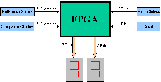
Figure 2: System-level Block Diagram
ASIC Requirements
The design consists of several functional blocks, each performing
a particular task. Figure 3 shows the internal components and the I/O
requirements of the ASIC.
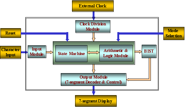
Figure 3: ASIC Modules and I/O requirements
The basic design consists of the above modules shown. The input
module takes the input character one by one with the help of a PB. It takes
first eight characters as reference string and next eight characters as
comparing string. For the next input characters this module works in the same
way. An external clock provides synchronization for the state machine
execution. The clock division module divides the clock to a lower frequency if
required.
The main module shown at the center of the diagram comprises state
machine and the arithmetic & logic module. This state machine collects the
input characters and based on the mode selected it sends the input data to the
arithmetic and logic module. In fact, the state machine generates control bits
that control the operation of all the other modules in the design. The
arithmetic & logic module performs the necessary mathematical and logical
operations on the data.
After the result of the selected function is calculated, the main
module sends signals to the output module (two 7-segment display controller).
The 7-segment controller/decoder module translates these signals and light up
the 7-segments to display the numerical result.
The
BIST (Built-In Self-Test) module lights up each of the LED’s and 7-segement
displays to verify their operation.
A one-pulse module was needed in the actual implementation to
remove the debounce effect of the two push buttons.
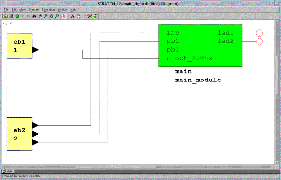
Figure
4: Block Diagram
of the Test Bench
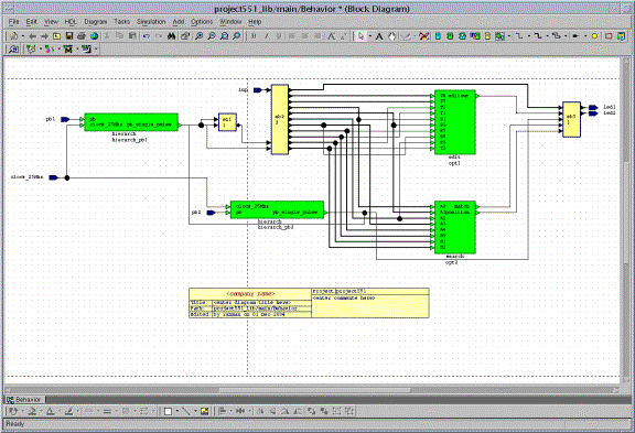
Figure
5: Block Diagram
of the Main Module

Figure
6: Block Diagram
of theEdit Module
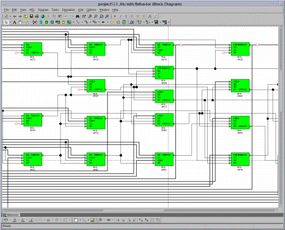
Figure
7: Zooming in to
the Block Diagram of the Edit Module

Figure
8: Flow Chart of
the Search Module
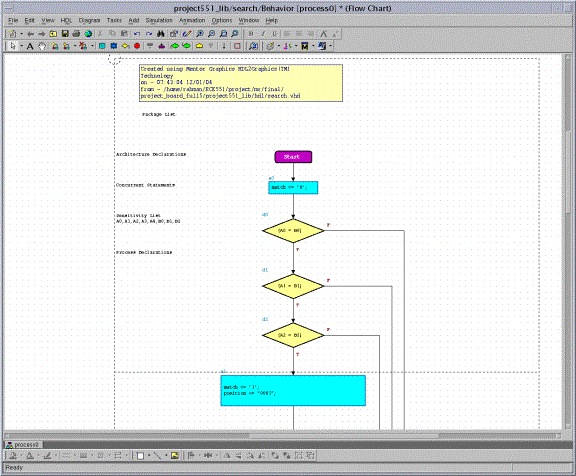
Figure
9: Zooming in to
the Search Module Flow Chart
Pre-Synthesis
Simulation Results
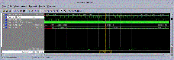
Figure
10: Test Bench
Simulation

Figure
11: Edit Module
Simulation

Figure
12: Search Module
Simulation
Figure
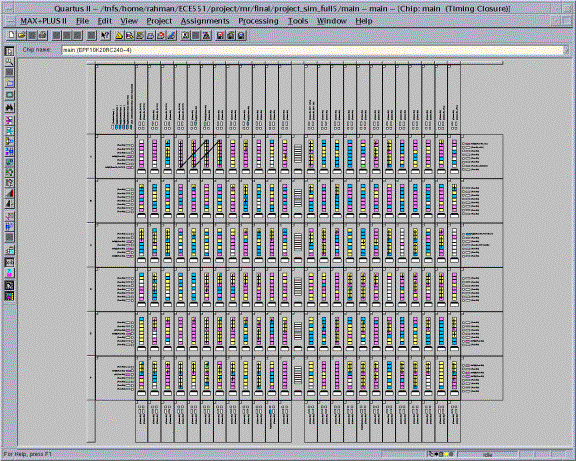
13: Floor Plan
for Altera FLEX 10K20
Figure
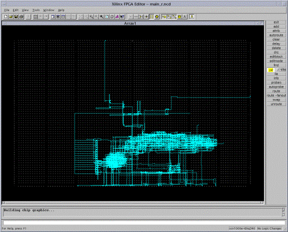
14: Layout in
Xilinx XCV1000E
Figure
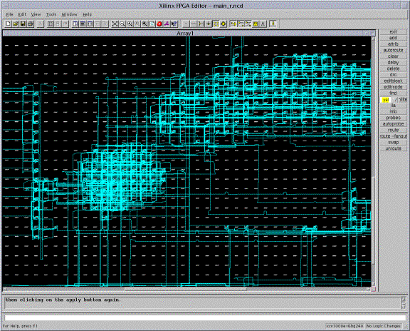
15: Zooming in to
the Virtex Layout
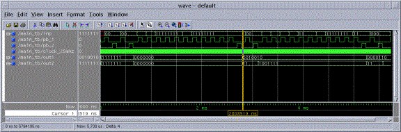
Figure 16: Test Bench Simulation
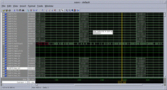
Figure 17: Edit Module Simulation
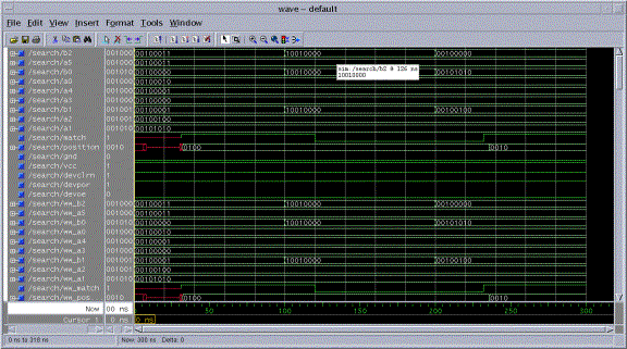
Figure 18: Search Module Simulation
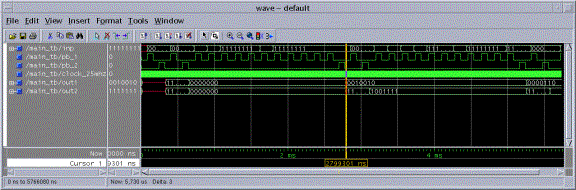
Figure 19: Test Bench Simulation in Virtex
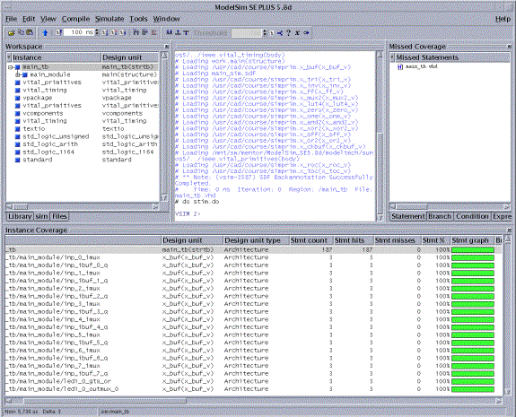
Figure 20: Post-Synthesis Coverage for Virtex
Implementation in the Altera
Tools
Since the function blocks were developed previously using technology-independent VHDL, they were resynthesized into a technology-dependent structural description using the Altera library. The system was coded in IEEE-compliant VHDL and compiled and simulated using the Altera MAX2PLUSWIN Suite. This provided an opportunity to detect and correct errors early in the design process. It also allowed each module to be individually simulated to verify correct operation before the entire system was tested.
The project file was downloaded to an Altera evaluation board containing a FLEX10K20RC240-4. This is a 240-pin FPGA, which had barely sufficient room to store the logic functions for this project. Several pins on the chip were hardwired to specific components on the evaluation board, such as seven-segments, LEDs, dip switches, etc. The eight Flex switches were used for entering the code corresponding to the input characters and the two Flex push buttons were used for mode control. The pin numbers for each device were available in the documentation for the board, and were manually assigned in the Altera software prior to downloading. Also, an external clock signal was used, and applied to another pin on the chip, which was then manually selected in the Altera software. The logic floor plan for the designed system has been shown here once again for convenience.

Figure
21: Altera logic floorplan
Before downloading to the Altera evaluation board we performed simulation for theoretically expected results using a test vector file. The simulation results were found satisfactory.
System performance
After successfully downloading the project to the evaluation board, a series of tests were performed using the physical inputs (switches and push buttons) and physical outputs (seven-segment displays) on the board. Edit distance calculation, substring search and other options were performed and correctly verified for many sets of data. The seven-segment LEDs functioned correctly for all the possible values.
The physical results corresponded exactly to the results predicted by manual analysis and software simulations. This confirms that the design process was complete and the implementation of the design was accurate.
Conclusion
The ‘String Comparator’ we designed and developed was successfully tested using an Altera FPGA device. General system functions were broken down into modules, which were designed and coded using VHDL. All the design objectives were met and hardware implementation worked perfectly. However, we could have allowed more characters per string and made the system work with strings of variable length. We also developed some codes and did some successful pre-synthesis simulation in order for supporting these enhanced features. However, when we tried to synthesize and place and route those functions, we found the Altera FLEX 10K20 device exceeding the maximum gate limit. We also had some problems implementing WHILE loops and WAIT statements. Therefore, we had to be a little defensive on coding and synthesizing attempts due to the hardware limitations. Otherwise, everything worked just fine. Of course, there is sufficient scope for enhancing the system and adding more features to it, especially with a larger capability FPGA device. It is also possible to implement our design in other technologies, such as Xilinx, because the design core is technology independent.
As a final point, it is worth mentioning some
features of the string comparator and edit distance measurements. The
Levenshtein distance algorithm has been successfully used in:
- Spell checking
- Speech recognition
- DNA analysis
- Plagiarism detection
- File revision etc.
As a whole, the lessons learned from working on this project were great and it provided us some insight in to FPGA design with real-life hands on experience.
[1] http://www.csse.monash.edu.au/~lloyd/tildeAlgDS/Dynamic/Edit/
[2] http://www.merriampark.com/ld.htm