Homework_3 -- Designing an 8-bit Adder Datapath

Revised 09/06/2010 by D. Bouldin
View (but do not execute) the USC Cadence Tutorial (html)
or (pdf)
to draw schematics and symbols
to implement a full adder as a single-bit slice.
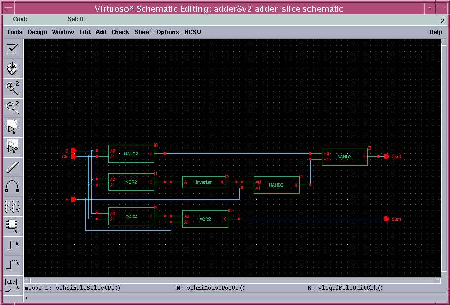
Develop your own full adder circuit schematic like the one below
(generate symbols or combine fet-level schematics from the OSU_FreePDK library):
Copy the layouts of these same std-cells from the OSU_FreePDK library and
edit them into a single-bit adder that adheres to the datapath library rules.
A possible topology is shown below:
     Vdd   GND    Vdd    GND    Vdd
     |      |      |      |      |
     | XOR  | NAND | XOR  | NAND |
     | p-n  | n-p  | p-n  | n-p  |
     | p-n  | n-p  | p-n  | n-p  |
     | p-n  |      | p-n  |      |
     | p-n  | n-p  | p-n  | n-p  |
     | p-n  | n-p  | p-n  | n-p  |
     | p-n  | NOR  | p-n  | NAND |
     |      |      |      |      |
     |      |      |      | INV  |
     |      |      |      | n-p  |
     Vdd   GND    Vdd    GND    Vdd
Your layout may be similar to this
one which was performed from scratch.
Include rulers in your layout.
A second example layout (2.44 H x 11.07 W) is here.
For the I/O, let Ai and Bi enter from the left on poly and SUMi exit
on the right on metal-2. The carry signals should align perfectly in
the vertical dimension as well as the Vdd and GND buses. You should have
room to also let the Carry-in enter each bit-slice on the left in poly and
the Carry-out exit on the right in metal-2. Only the LSB Carry-in and the
MSB Carry-out need to be connected externally when you simulate the 8-bit adder.
Array the single-bit adder into an 8-bit datapath (both
schematic and layout).
Include rulers in your layout.
Simulate the design for the single-bit and 8-bit implementations using HSPICE
(both pre-layout and post-layout) with the following inputs:
Set all eight A inputs to 1 and all eight B inputs to 0.
Then, apply the same type input as in hw2 to the Carry-in input on the LSB:
pwl wave=[0n 0 1n 0 1.5n 1.1 3n 1.1 3.5n 0 6n 0]
Run the simulation until the SUM and Carry-out outputs settle (20 ns or more):
tran1 tran start=0 stop=20n step=0.05n errpreset=moderate
Measure the delay between the mid-point on the LSB Carry-in input
to the mid-point on the MSB Carry-out output.
Post your results for both the single-bit and the 8-bit simulations.
Link your results to your web home page.
Update hw.html
dbouldin@tennessee.edu