Computer Aided Design of VLSI Systems IIECE 652 PROJECT REPORTTeam - Advanced Encryption Standard (AES) IP BlockRishi Raj Srivastava, Nitin TiwariApril, 2002 Electrical
& Computer Engineering
University of Tennessee Knoxville, TN 37996 Contents
1.0 AbstractThis project is a part of a System on Chip (SoC) project being implemented as a one large team class project.Our part in the project involved testing of the Advanced Encryption Standard Cipher - Inverse Cipher core obtained from www.opencore.com,Targetting it the Core for Xilinx 1000e (FPGA) and TSMC 0.18 6 metal ASIC. Once that was done we added Synopsys DesignWare RAM for reading the Key and Data for the Cipher and writing out the Ciphered text. The whole RAM-Core-RAM system was then simulated and synthesized and Placed and Routed targeting the FPGA and ASIC mentioned above. The IP block with the RAM was then wrapped around a wrapper to connect it to the AMBA bus then had to be placed in the SOC. 2.0 Introduction to Advanced Encryption Standard (AES)AES is the latest Federal Information Processing Standard (FIPS). AES is implemented
using the Rjindael(read- rhinedahl) Algorithm. The 'Rjindael' algoritm was designed
by Joan Daemen and Vincent Rijmen from Belgium. Rjindael is a block Cipher that
takes in Key and input text in variable bit block lengths. The current version
can have 128,196,256 bit Key to cipher data with block length of 128,196,256
with all the nine combinations possible. Rjindael algoritm's combination of
Security, Performance, Efficiency, Ease of implementation and flexibilty made
it the best choice for being AES. It has a Round Permutation Module that can
be looped 10, 12 or 14 times, further enhancing its ciphering capabilities.
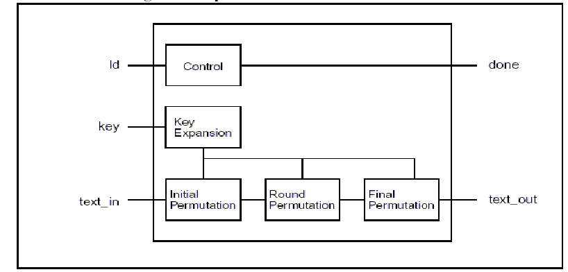
3.0 AES Cipher
The AES cipher core consists of a
key expansion module, an initial permutation module, a round permutation module
and a final permutation module. The round permutation module will loop internally
to perform 10 iteration (for 128 bit keys). 4.0 Task Requirements Our two member sub-team was required
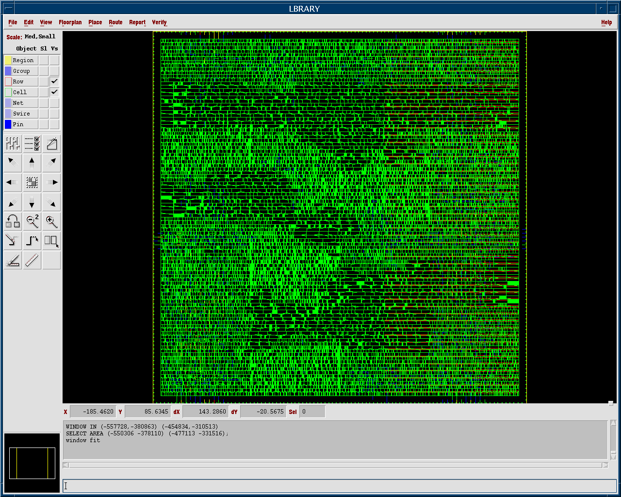
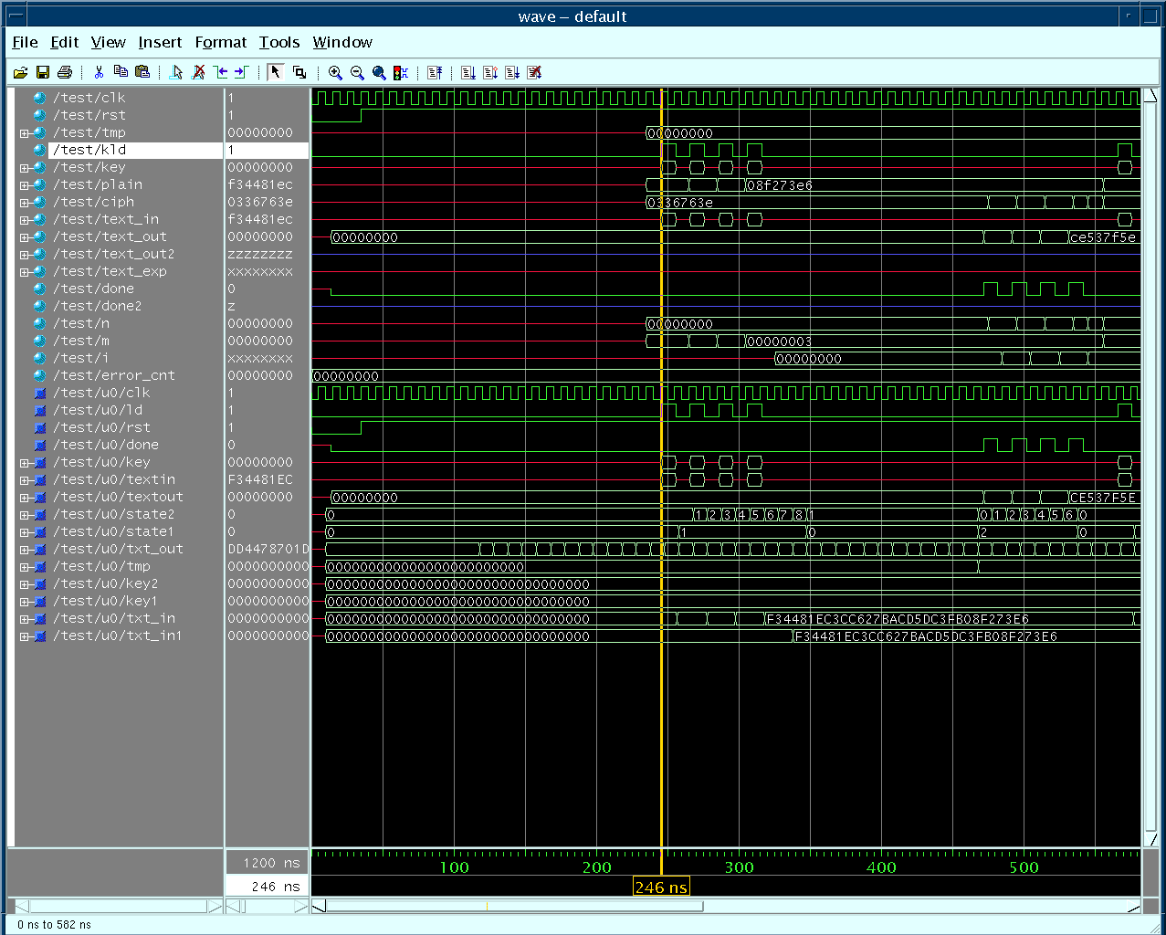
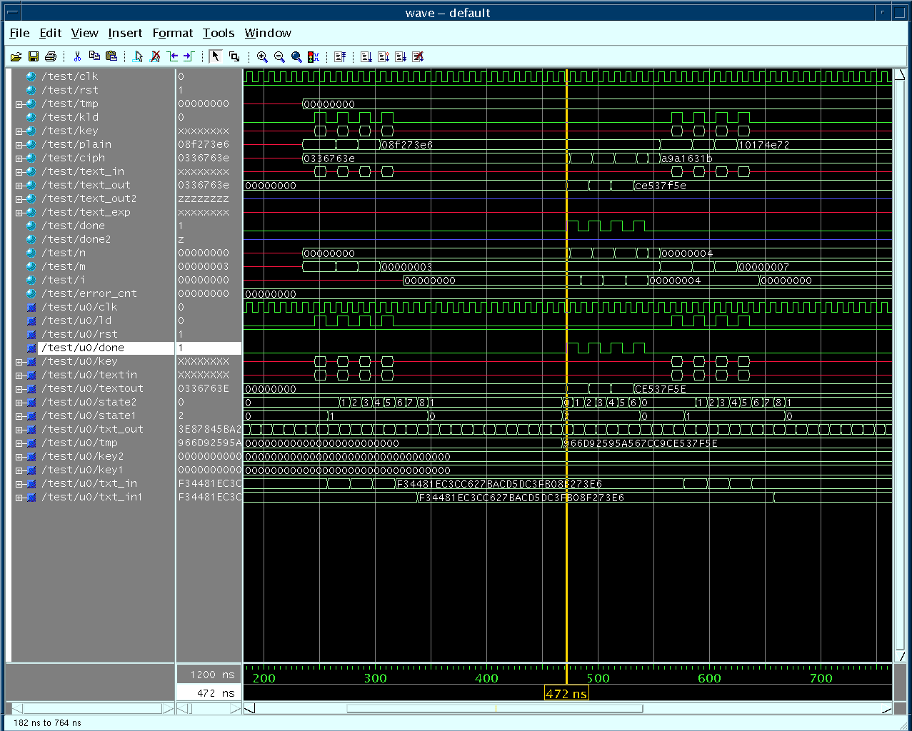
to complete these tasks : 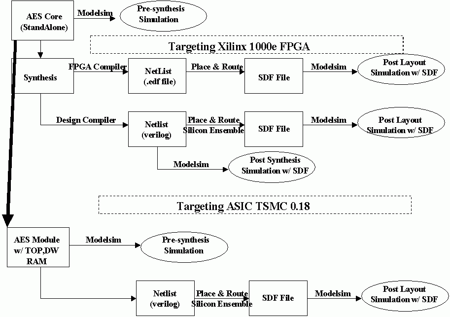 Figure 2. Process Flow 5.0 Implementation Steps and Methodology1. The AES core was obtained from opensources.com. The core is basically two parts. The AES Cipher top and the AES Inverse Cipher top. The core comes along with a Verilog TestBench. The test bench supplies the Key, Plain Text and Ciphered data (to cross-check simulation results) in blocks of 128 bits. 2. The first thing that was done with the core obtained was pre-synthesis simulation on the Cipher-Inverse Cipher core using the TestBench provided along with it. 3. Once that was done the core was then synthesized targetting ASIC tsmc 0.18 technology on the Design Compiler and then Place and Route (P&R) performed on the synthesized Net-List using Silicon Ensemble. The SDF (standard delay format) file was obtained after P&R was done. This file along with the synthesized Net-List were used to perform Back Annotation Simulation (Post-Layout Simulation) on the stand alone core. Besides that Gate Level Simulation was done using the synthesized NetList without the SDF. 4. The Stand Alone
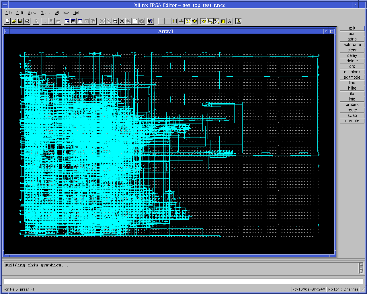
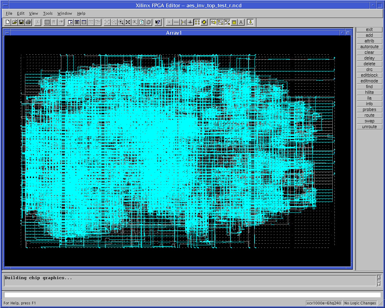
core was also synthesized targetting the Virtex 1000e FPGA part using the FPGA
Compiler fc2. But there was a resource constraint that we faced with the Input/Output
pins . We had to overcome this limitation by writing a Top over the AES
Cipher top to input data (Key and Plain text) as 32 bits and then collect that
data to form 128 bit Key and Plain text blocks. The Top has a State machine
that is synchronous in nature and is used to get data in blocks of 32 bits and
then appending these 32 bit block to form a 128 bit block of data. The Top proved
to be helpful when RAM was attached to the Cipher core as the RAM has a width
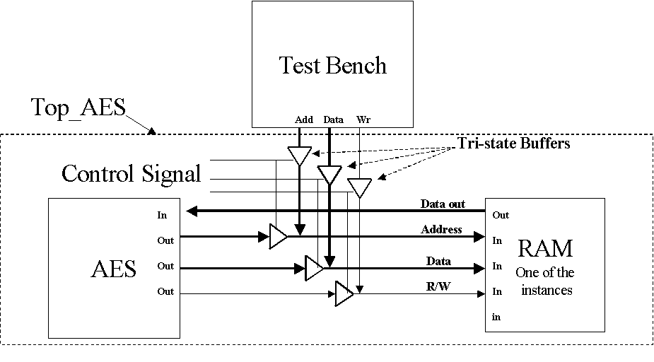
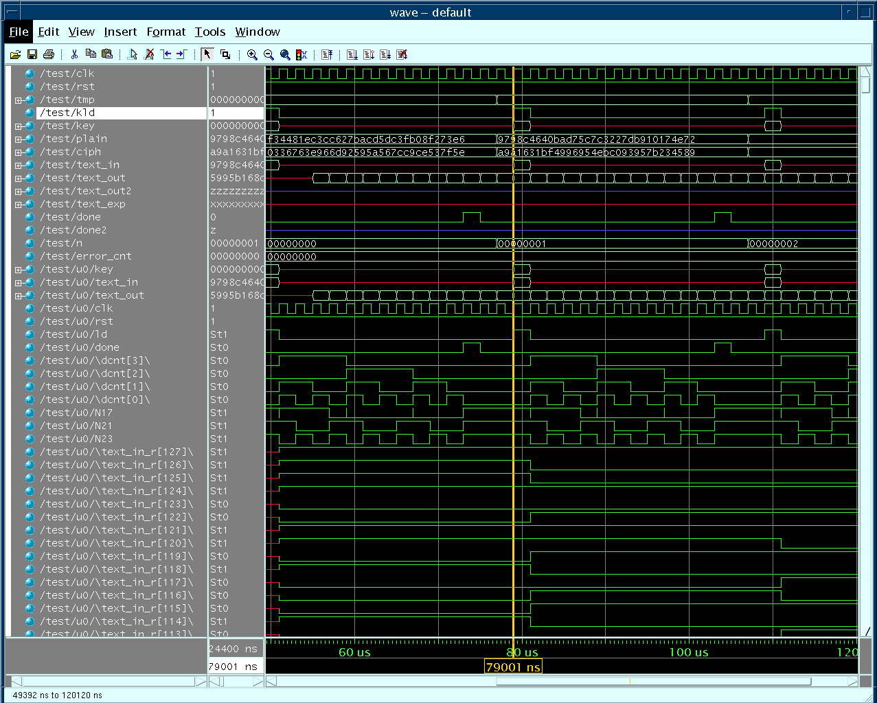
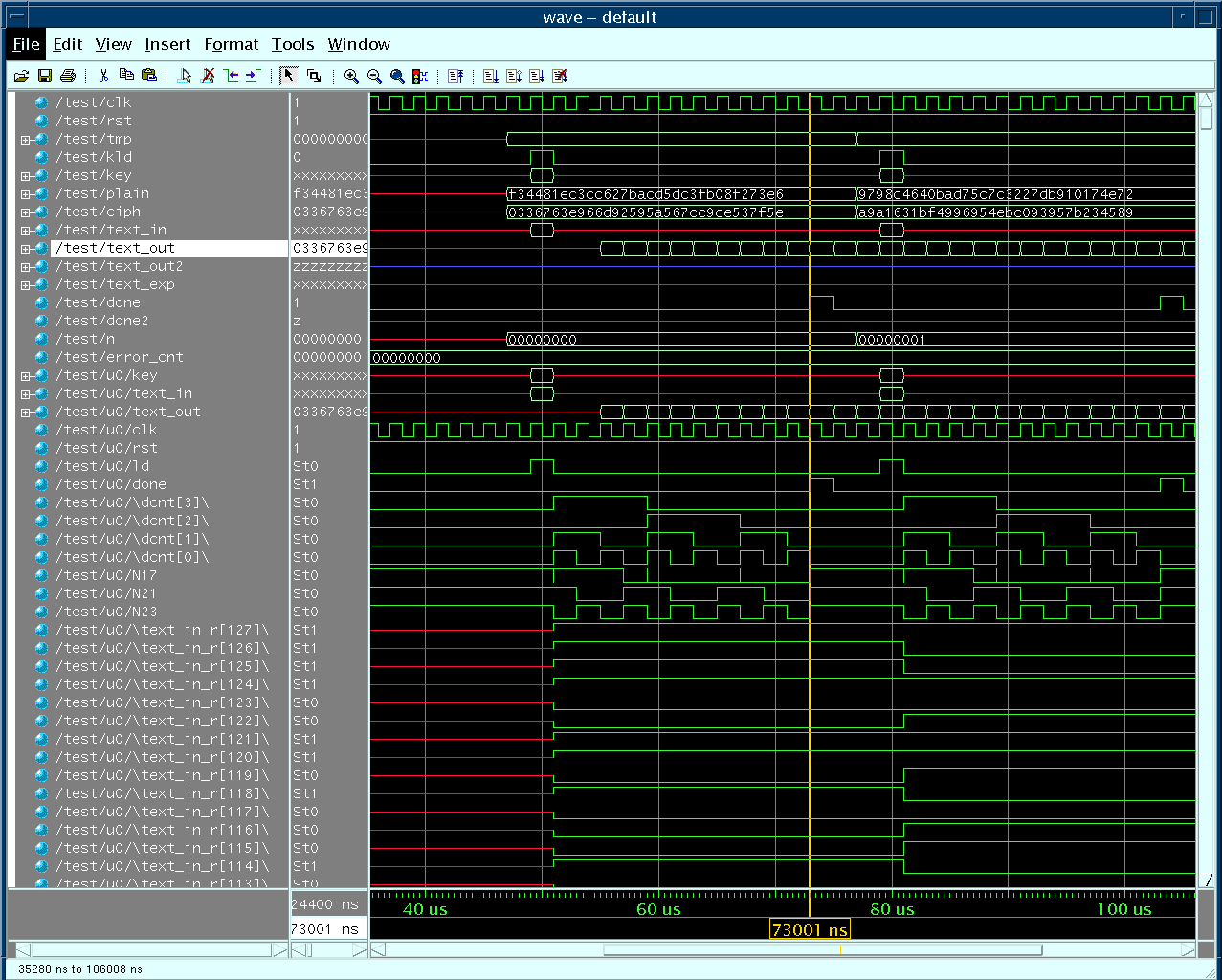
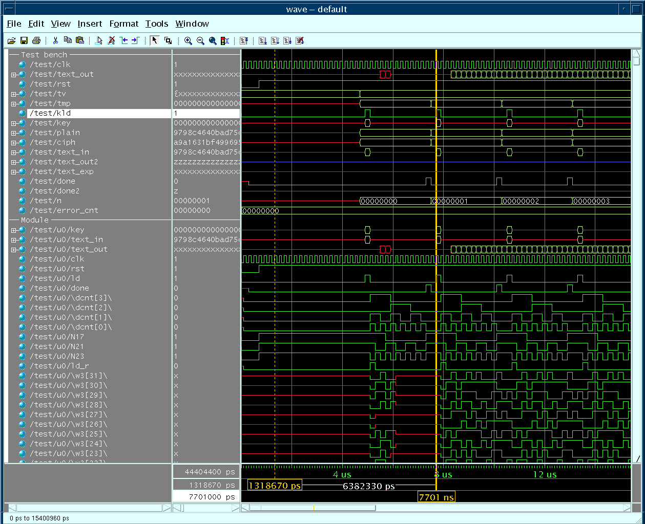
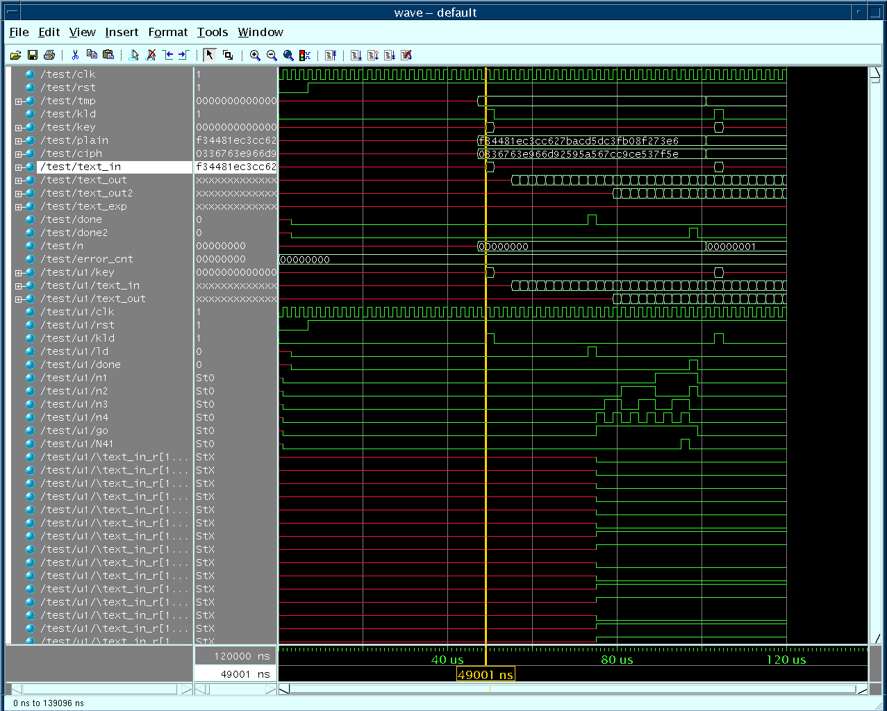
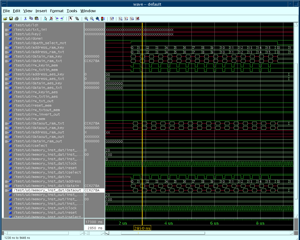
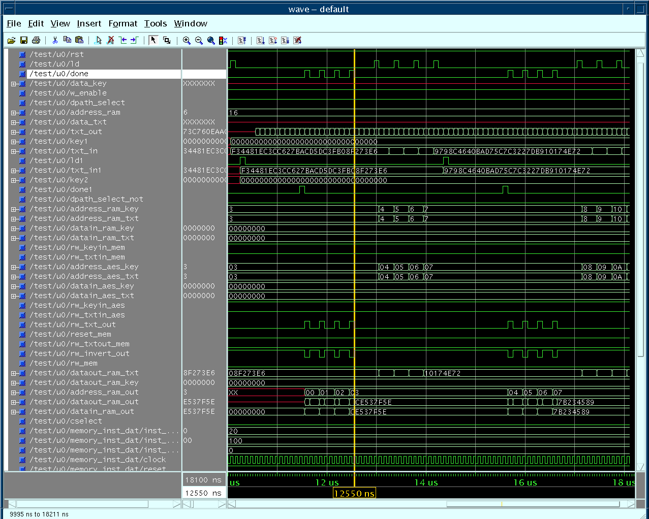
of 32 bits only to store any data. 5. After the standalone tests were done DesignWare RAMs were added around the Top made for 32 Bits of Input. There are three RAMs . One for storing the Key, one for the Input plain Text and the third one for storing the Output Ciphered text. The ram stores one block of 128bit Key/Plain Text in 4 locations of 32 bits. 6. To test this setup (RAM-Core-RAM) the test bench had to write to the RAM and then the Top had to read 28bit Data from the RAM and build up the 128 bit block. This firstly required modification of the Test bench to feed in 28bits of data instead of 132 and then a mechanism was required to pass the control of bus from Test Bench to the main Cipher Core. The mechanism used was a set of Tri-State buffer (described below). 7. Once the TestBench, Tri-State Buffers and the DW RAM were all intergrated, PreLayout simulation was carried out. 8. Synthesis was performed targetting ASIC TSMC 0.18 technology. Due to the large size of the design the RAM-Core-RAM design couldnt be targetted for the Virtex 1000e FPGA. Place and Route was peformed using the netlist on SE Ultra. The SDF file that was generated was used for back annotated simulation. 6.0 Top & The State Machine implemented in the TOP design
The AES Top that we wrote in VHDL is important in many ways: We are using Synchronous Single-Port, Read/Write RAM (Flip-Flop-Based)
DW_ram_rw_s_dff from Synopsys. The RAM-CORE-RAM implementationfor
the AES Cipher has been done using 3 instances of the above RAM. Two
of the RAMs are being used as Input RAMS for storing the KEY and the
Plain Text while the third RAM is being used to store Output Ciphered
Data. Since the RAMs are synchronous, data is being read on the rising
edge of the clock. Figure 3 shows the test bench block interaction in which tri-state
buffers are placed on the address, data (Key and Plain Text), and
read/write lines controlling the memory. During the first stage, the
tri-state buffers give control to the test bench. This allows the
test bench to read in the Key and the plain text to be ciphered and
write them into the DesignWare RAM. When the Key and text have been
read into the DW RAM, the control is switched to the AES Cipher side
so that it can read the Key and the Plain text and then cipher it
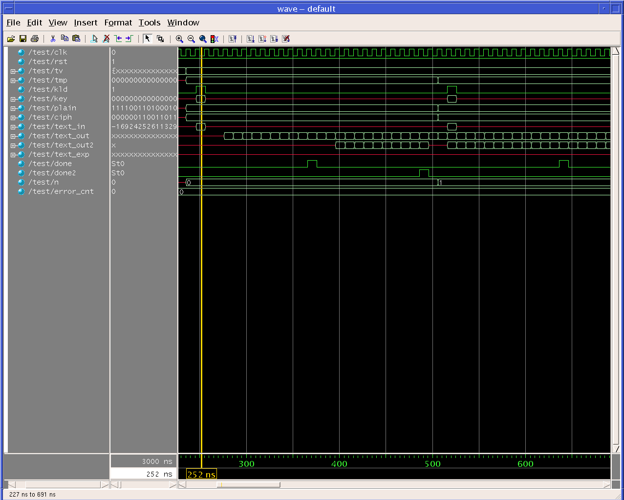
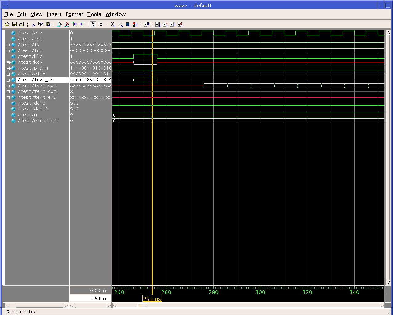
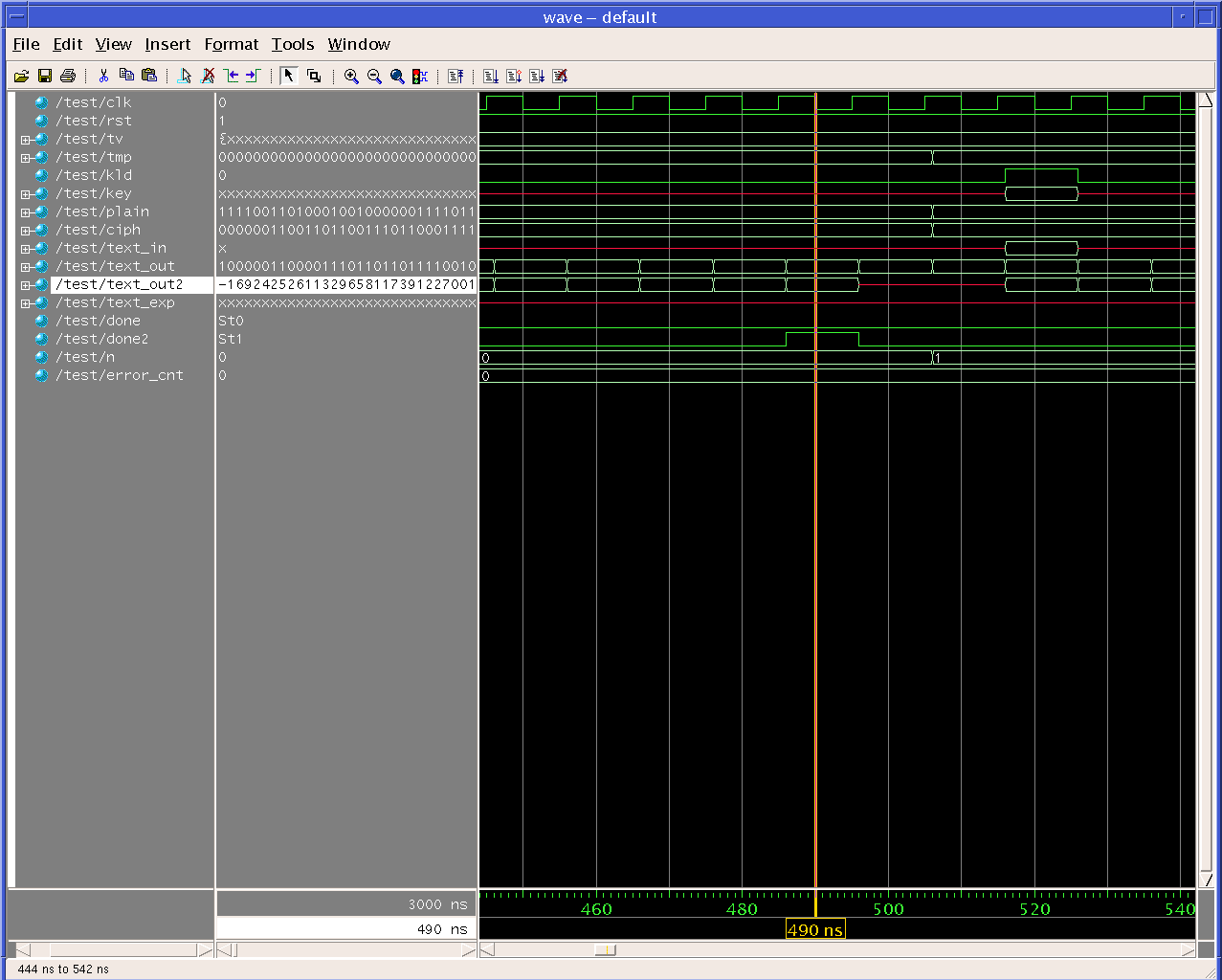
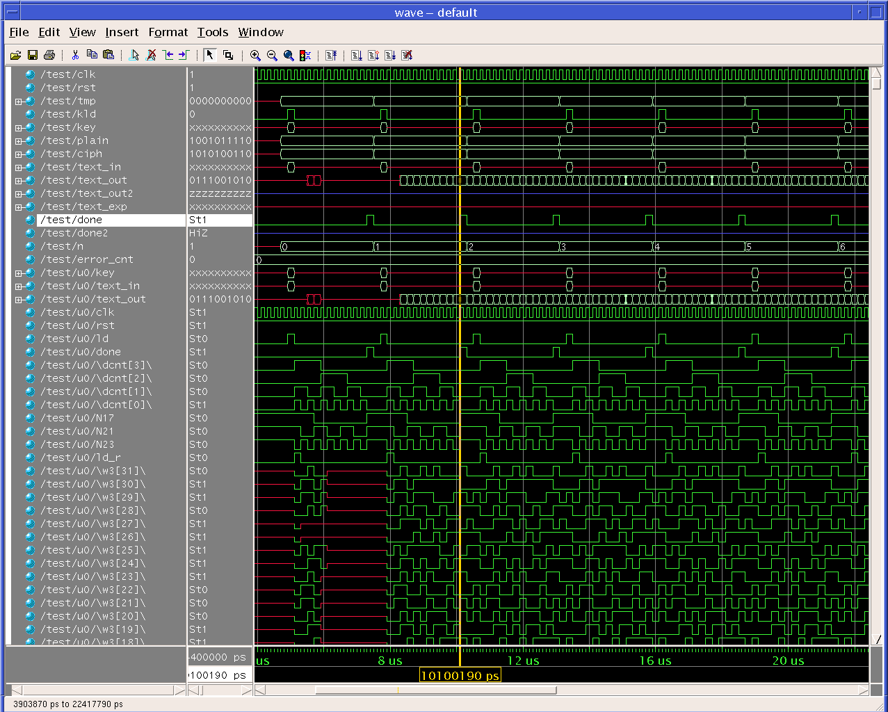
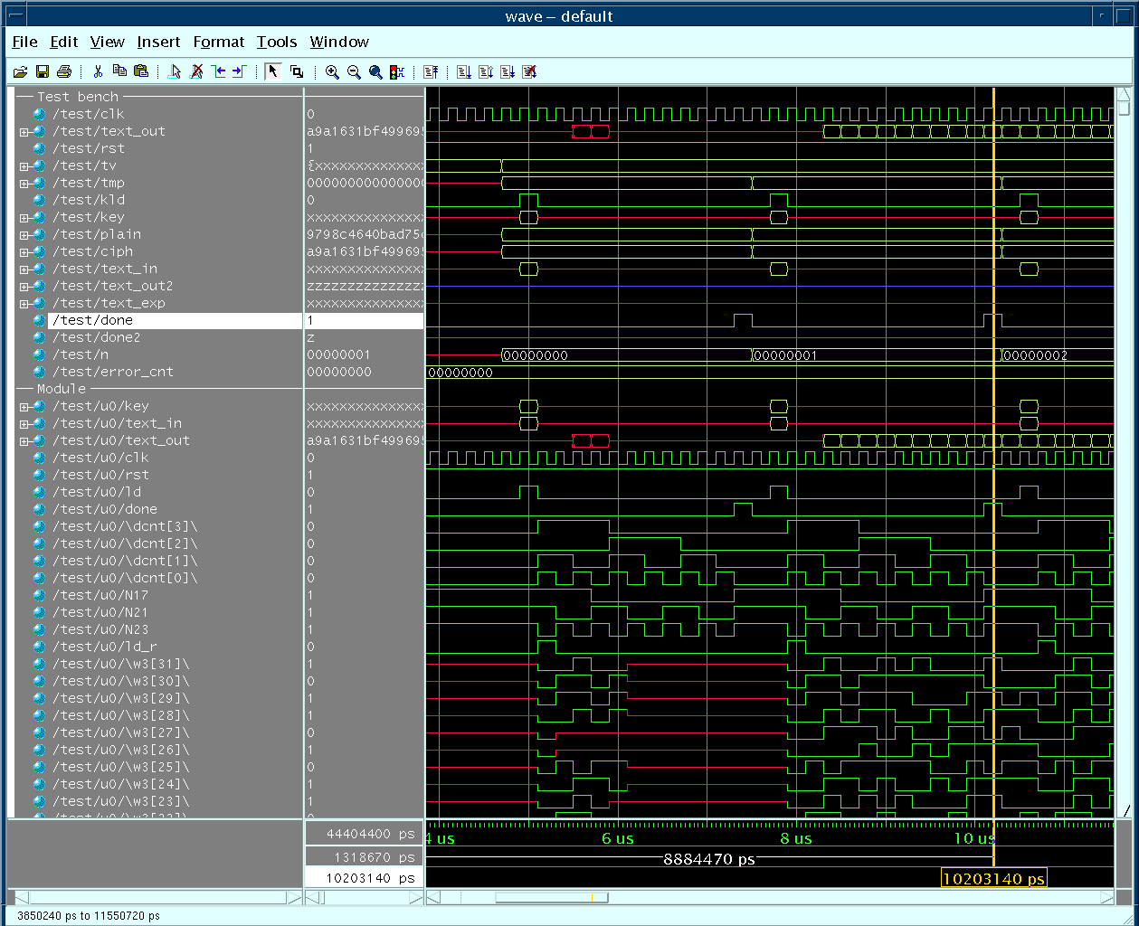
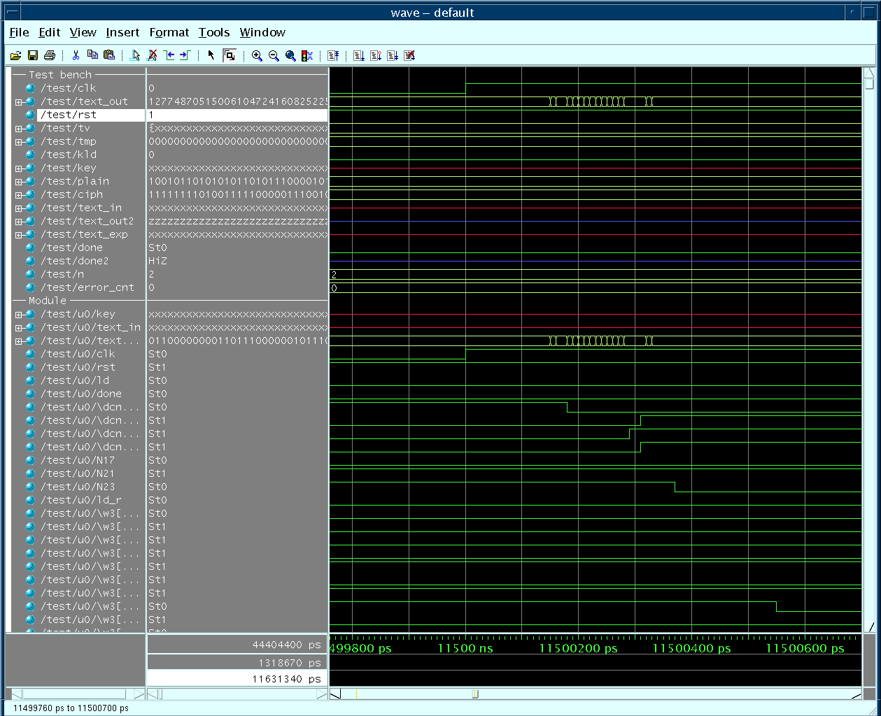
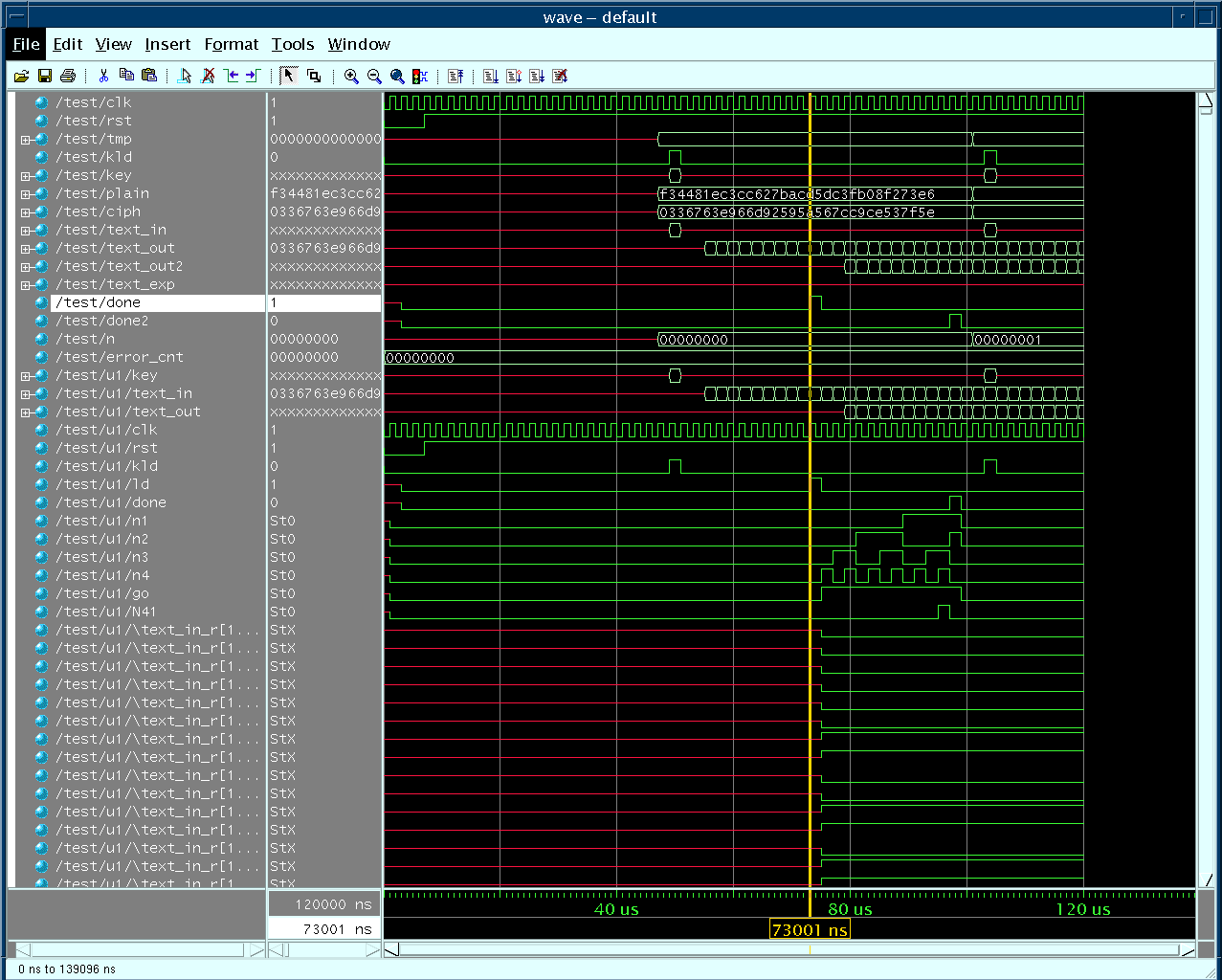
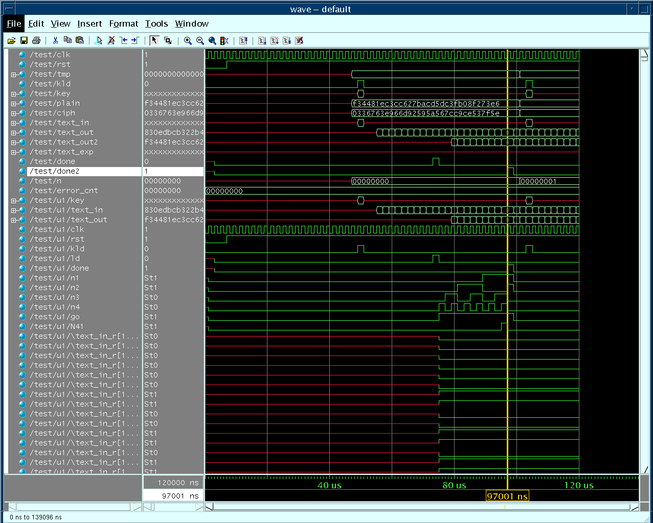
to encripted text. 9.0 Results9.1 Standalone AES Core ImplementationStandAlone PreSynthesis Simulations
: Performed on the core using the Test bench originally supplied
with the Core StandAlone AES Simulations and layout Xilinx Virtex 1000e ASIC TSMC 0.18 10.0 Summary and ConclusionsThe Project involved taking up a AES Core and testing it Standalone and then integrating it with a DesignWare RAM and testing aiming at FPGA(Virtex 1000e) and ASIC (tsmc 0.18) in both cases. The standalone design passed through easily through both the technologies. The RAM-Core-RAM system will not go through synthesis and P&R for the FPGA due to its large size. The RAM-CipherCore-RAM went through synthesis and we got simulations but when the whole system was placed and routed on Silicon Ensemble and a Post layout Simulation done using the SDF file there are some problems with the simulation. We have tried over and over again to get it but have not been able to get a fully correct output.
11.0 References and AcknowledgementReferencesWe would like to thank Dr. Don Bouldin for his guidance. Also, the students who worked with us in this project. Also would like to acknowledge the help we got from Dr. Chandra Tan. |