Sigma-Delta Modulator
Final
Report
By,
Stephen
C. Terry
&
Nazmul
Islam
For
the Course ECE 652
Course
Instructor: Dr. Don Bouldin
Date: 6th May 2003
Introduction:
Sigma-delta
modulation techniques have been very successfully used in analog-to-digital
conversion (ADC) applications over the last two decades. Although sigma-delta
concepts existed since the middle of the century, only recent advances in VLSI
technologies have made possible the appropriate handling of the bit stream
generated by the 1-bit ADC.
Although
now almost universally known a sigma-delta converter, these devices are
still referred to by some manufacturers as delta-sigma converters. This
term may be more appropriate in that, in its basic form, the converter
consisted of a delta modulator (used for many years in
telecommunications), where the input signal is added to the input of the
integrator instead of its output (thus eliminating the need for an integrator
at the receiver end) [1]. Unfortunately, with time the words delta and sigma
seem to have been interchanged arbitrarily. Nowadays, a distinction seems to be
made only when the relative position of the summing (sigma) block within
the modulator is being emphasized. In addition to the above, other terms often
found in the literature are over-sampling and noise shaping ADCs.
The
last two terms are in fact evocative of the two basic principles involved in
the operation of sigma-delta ADCs – over-sampling and noise shaping. The
former spreads the quantization noise power over a bandwidth equal to the
sampling frequency, which is much greater than the signal bandwidth. In the
latter, the modulator behaves as a low-pass filter on the signal, and as a
high-pass filter on the noise, thus "shaping" the quantization noise
so that most of the energy will be above the signal bandwidth. A digital
low-pass filtering stage then greatly attenuates out-of-band quantization
noise, and finally, down-sampling brings the sampled signal to the Nyquist
rate.
Sigma-delta
ADCs are very extensively documented in the literature. The emphasis, however,
seems to be either on very theoretical aspects involved in the technology, or
on the traditional low-speed, high-resolution applications of these converters.
A
very complete review of oversampling methods used for A/D and D/A conversion,
as of 1992, is presented in [1]. The paper [2] also provides an up-to-date view
of the technology, including an examination of its use in the A/D conversion of
narrowband bandpass signals, as well as a discussion of several parallel
architectures.
Advantages and
disadvantages of sigma-delta ADCs
The
penalty paid for the high resolution achievable with sigma-delta technology has
always been speed - the hardware has to operate at the oversampled rate, much
larger than the maximum signal bandwidth, thus demanding great complexity of
the digital circuitry. Because of this limitation, these converters have
traditionally been relegated to high-resolution, very-low frequency
applications (Figure 1), and more recently speech, audio and medium speeds (100
kHz to 1 MHz).
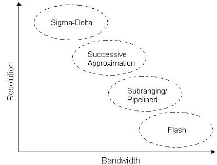
Figure
1: A/D Converter
technologies, resolution and bandwidth
The
digital filtering stage results in long latency between the start of the sampling
cycle, and the first valid digital output; similarly, there is a significant
lag thereafter between digital outputs and their corresponding sampling
instants. This characteristic has prevented the use of these converters in
multiplexed systems - it takes many clock cycles for the digital filter to
settle after switching from one channel to the next.
By
having thus outlined the key limitations of these devices, we've established
the framework within which they are suitable, and may now proceed to itemize
their numerous advantages when compared with alternate technologies:
- Most of the circuitry in sigma-delta converters is digital. This implies that performance will not drift significantly with time and temperature. Also, incorporation of the converter into a single-chip package with additional circuitry, such as a D/A converter (Codec), microcontroller, or DSP is feasible. Finally, the cost of implementation is low and will continue to decrease.
- They are inherently monotonic (i.e., a change in the digital output has always the same slope as the analog input). This is of particular importance in closed-loop control systems, where misinterpretation of the direction of change of a measured variable may cause the system to become unstable.
- They are inherently linear, and present little differential non-linearity.
- They do not require an external sample & hold circuit; due to the high input sampling rate and low precision of the A/D conversion, the devices are inherently self-sampling and tracking.
- Requirements for analog anti-aliasing filters are minimum - in most cases, a simple single pole RC-filter suffices. In contrast, the filters required for medium- to high-resolution applications using other (non-oversampling) technologies are very sophisticated, difficult to design, large, and expensive.
- The background noise level, which determines the SNR, is independent of the input signal level.
- Since there is a digital filtering stage after the A/D converter section, noise injected during the conversion process can be controlled very effectively. In fact, the filter may be tailored to minimize noise with very specific characteristics (e.g., 60 Hz).
- As stated above, their mostly digital nature makes these devices relatively inexpensive. In multichannel applications, a one-converter-per-channel architecture will often be more cost-effective than a single (very fast, non-oversampling) converter with multiplexed inputs.
Modulator architectures and implementation problems
The structure of the basic first-order
sigma-delta converter is shown in Figure 2. The modulator consists of an
integrator and a comparator, with a 1-bit DAC in a feedback loop. The
digital decimator that follows performs both, digital filtering and
down-sampling of the 1-bit input data stream.
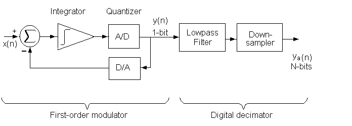
Figure 2: First sigma-delta A/D converter
Descriptions of the operation of this
converter, both in time and frequency domains, abound in the literature (see
for example [1], [2], [3]). The nonlinear nature of the devices makes precise
analysis difficult, especially when higher order architectures are used; in
fact, in many cases behavior has only been possible to characterize through
simulations. Here we limit ourselves to a brief discussion of common variations
of the basic architecture, and implementation problems that might be expected.
Even
the very simple first-order modulator can achieve very attractive SNRs; a good
"rule of thumb" is that for every doubling of the oversampling ratio,
the SNR will improve by approximately 9 dB [2]. In this architecture,
imperfections in the integrator usually don't present significant difficulties,
unless the oversampling ratio is extremely large. Similarly, constraints on the
accuracy of integrator and DAC gains are quite lax - typically, the gain is
implemented as a ratio of two capacitors, and the precision required in their
matching is of only 1 part in 10. With regard to the quantizer, we observe that
any noise introduced by nonlinearities is subject to noise shaping by the
modulator, and has therefore little effect on SNR.
A
significant problem with the basic first-order system, resulting directly from
its nonlinear nature and feedback, is the presence of limit cycle oscillations.
This will produce periodic or "tone" components in the output in
response to DC inputs, or even small amplitude sinusoidal inputs. Clearly,
these tones are highly undesirable in audio/speech applications; for this
reason, even when the overall SNR may be very good, first-order modulators are
practically never used in these areas.
Conceptually,
the extension to a second-order modulator is quite straightforward. By
incorporating a second integrator more quantization noise is "pushed"
outside the passband. In this case, every doubling of the oversampling ratio
results in a 15 dB increase in SNR.
With
two integrators, we are now concerned with the accuracy of both their gains.
Fortunately, it has been shown [2] that these are (relatively) insensitive to
deviations from their nominal values over quite a wide range of oversampling
ratios. The problem with limit cycles remains however, resulting in idle tones
for DC or low amplitude sinusoidal inputs; also, unlike in the first-order
case, the limit cycles are now dependent on the initial condition of the
output. Furthermore, an additional potential problem with a second-order
modulator that uses a single-bit quantizer, is that of "overloading";
this may produce harmonic distortion tones for sinusoidal inputs, as well as
significant tone components near fs/2.
In
addition to further improving SNR, higher than second-order modulators will
also alleviate some of the problems with idle tones. In general, for an N-order
modulator every doubling of the oversampling ratio provides an additional (6N
+ 3) dB of SNR. A great variety of topologies have been implemented [1,2], and
very often these are patented by the manufacturers. Clearly, the complexity of
the circuitry increases dramatically, (conditional) stability is harder to achieve,
and exact analysis is seldom possible.
Higher-order modulation can also be
achieved by cascading several lower-order stages. This avoids problems with
stability, while maintaining the advantages with respect to SNR and limit
cycles. Fourth-order modulators consisting of the cascading of two second-order
stages are common.
There
are also architectures that employ multi-bit quantizers. For example, in a
second-order modulator, each additional bit in the quantizer results in a SNR
improvement of about 6 dB. The stability of these systems is easier to predict
(since a linearized model will more accurately represent the system), and idle
tone problems are also alleviated. On the other hand, because of the linearity
required for high-resolution converters, the multi-bit DAC is more difficult to
fabricate.
Overview
of Sigma-Delta Converter Development in 1.8V/0.18mm CMOS
Implementing an analog or mixed-signal system
in a 1.8V digital CMOS technology poses many challenges. First, the low power
supply voltage means that dynamic range is at a premium. In this work several
steps were taken to ensure robust operation at low voltages, including the use
of dynamically biased low voltage cascode current mirrors (LVCCM) in the
integrator. The second major design challenge is that this technology does not
include linear capacitors as an option. Linear capacitors are extremely
important in many data converters because they form the backbone of
switched-capacitor circuits. The most common application of switched-capacitor
circuits in sigma-delta data converters is in the integrator. Considering that
linear capacitors were not available, it was decided that a continuous-time,
current-mode integrator would be used instead of the more traditional
switched-capacitor integrator. The main advantage of the current-mode
integrator is that it possible to bias the integrator such that the gate
capacitance of a MOSFET can be used as a linear capacitor. Thus, a high
performance sigma-delta converter can be realized in a digital CMOS technology
that does not have linear capacitors.
In order to further investigate sigma-delta
data converter develop in a deep sub-micron, digital CMOS process, the critical
components used in a sigma-delta have been laid out and simulated and are now
ready for fabrication. These cells include a non-overlapping clock generator,
high-performance clocked comparator, and a current-mode integrator. The next
step in the development process is to fabricate and test these individual cells
to insure that their performance is adequate for the sigma-delta requirements.
Additionally, during testing it will be possible to build a sigma-delta
converter out of the fabricated components, and thus the performance of the
complete converter can be evaluated.
Comparator Design:
Comparators are a key component in a data-converters because they represent the link between the analog and digital domains (i.e. analog signal in and digital level out). To get an efficient Sigma-Delta Converter we need a high-speed comparator with high resolution. This comparator can achieve 8-b accuracy with sampling rate up to 65 MHz.
It consists of a differential input pair, a CMOS latch
circuit (both n-channel and p-channel flip-flop) and an S-R latch (generates
CMOS compatible output voltage). We have used two non-overlapping clock named
S1 & S2 in the circuit. To generate the non-overlapping clock the clock
generation circuit was also generated.
After doing the pre-layout
simulation, the post-layout simulation was done. Pre-layout give a delay of
97.6 pico-sec, on the other hand the Post-layout gave a delay of 104 pico-sec. The reason behind the high
delay in post-layout simulation is there creates extracted capacitance in the
post layout simulation.
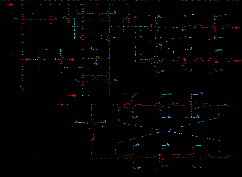
Figure 3: Schematic of Comparator
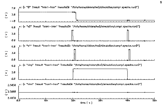
Figure 4: Pre-Layout Simulation of Comparator
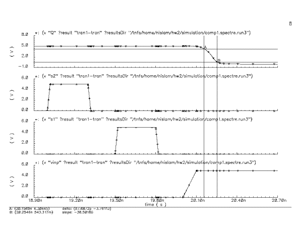
Figure 5: Zoomed Pre-Layout Simulation of Comparator
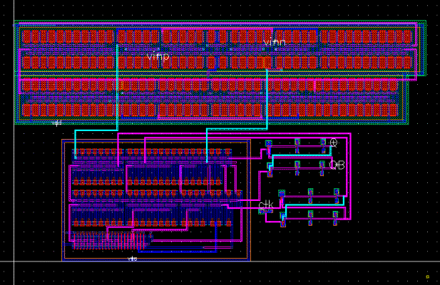
Figure 6: Layout of the Comparator
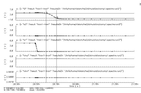
Figure 7: Zoomed version of Post-Layout Simulation of Comparator
Integrator Design:
The integrator is perhaps the most important component in a sigma-delta converter because it determines the noise floor and dynamic range. As stated previously, it was decided in this project to use a current-mode integrator because linear capacitors are not available in this technology. If linear capacitors were available, a switched capacitor integrator would be used. Figure 8 presents the integrator schematic, which is based on the integrator presented in [4]. Notable in this implementation is the cascode operation at 1.8V power supply, which is facilitated by the dynamically biased NMOS cascode current mirrors. Additionally, the bias current for each leg of the integrator is 100mA. Figure 9 presents the Smartspice simulation for the integrator. One can see that the integrator has a finite DC gain of roughly 50dB with a dominant pole at 10 kHz. The integrator layout is shown in Figure 10. Notable in the layout is the extensive use of common-centroid symmetry. Finally, Figure 11 presents the Smartspice simulation for the post-layout extraction of the integrator. As one can see, there is very little difference between Figures 9 and 11.
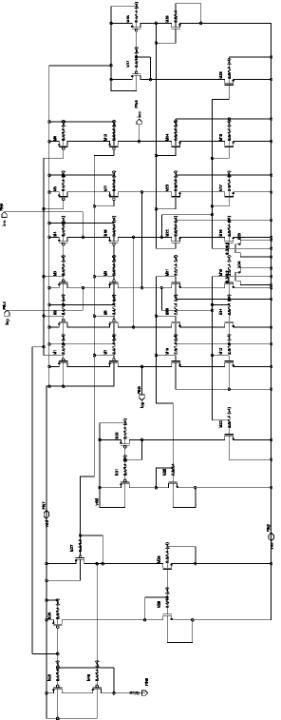
Figure 8: Cadence Schematic of Current-Mode Integrator
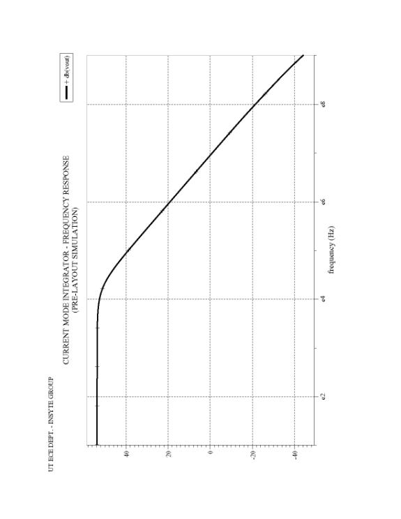
Figure 9: Pre-Layout Simulation of Current-Mode Integrator
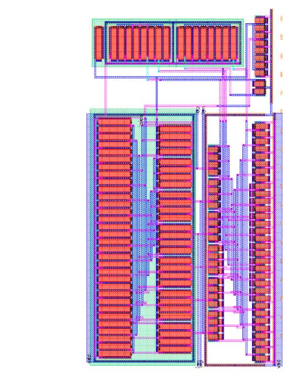
Figure 10: Integrator Layout in 0.18mm CMOS technology
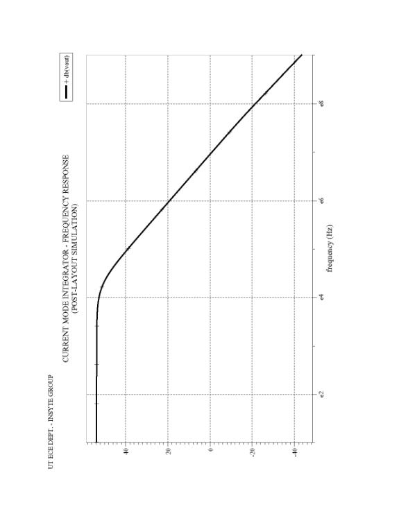
Figure
11. Post-Layout Integrator Simulation
Conclusion
We have presented the design, layout, and
simulation of components required in a sigma-delta data converter. These cells
are now ready for fabrication and testing. The most notable aspect of this
design is that all cells have been operate at 1.8V, and no cell requires linear
capacitors. The next step in this work will be to measure the actual
performance of the different system components and make any adjustments that
necessary so that this work can be targeted to a SOC.
References
[1] J. Candy and G. Temes, "Oversampling methods for A/D and D/A conversion," in Oversampling Delta-Sigma Data Converters, pp.1-25, IEEE Press, 1992.
[2]
P.M. Aziz, H.V. Sorensen and J. Van Der Spiegel, "An overview of
sigma-delta converters," IEEE Signal Processing Magazine, Vol.13,
No.1, Jan. 1996.
[3] Analog
Devices, "Sigma-delta conversion technology," DSPatch - Digital
Signal Processing Applications Newsletter, Winter, 1990.
[4] R.H. Zele and D.J. Allstot, “Low Power CMOS Continuous-Time Filters,” IEEE J. Solid-State Circuits, vol. 31, no.2, Feb. 1996, pp. 157 – 168.