Figure 1: Creating library and Attaching the tech library
Objective: After finishing this lab students can design bigger circuits. They will also be more familiar with the Simulations.
Login to UNIX system to do this lab. After login to UNIX you are in your home directory. "cadence" is the directory where all of your cadence file should run
cd cadence
source /usr/cad/.cshrc
cadence_tools
icfb&
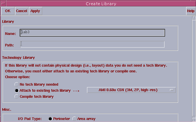
Go to the Library Manager. Now make your own library where you will draw your schematic. You can do this in two ways, first you can create a new library from the Library Manager, or the CIW. In either case select File->New->Library. This will bring up a new window. Enter the name of the new library (lab3), and select Attach Existing Library (AMI 0.6u C5N). [Like figure1]. When there is no path entered, it will place the library in the directory from which you started Cadence.
Figure 1: Creating library and Attaching the tech library
Next stages will be creating a New Cell View, Drawing Schematic, Symbol and doing Simulation with Spectre.
Under Grad Students will do Either NAND or NOR gate.
Graduate Students will do XOR gate
Follow the Princeton tutorial to draw a schematic of an inverter using
the ami06 library. Use the Tutorial link http://analog.ece.utk.edu/Cadence/utk_schematic.htm
Note that for the AMI-0.6 process in which lambda = 0.3 micron. So
L = 2*lambda = 0.6 micron = 600nm.
Assume width, W = 3.0 micron. So W/L = 3.0/0.6 = 10/2. Learn how to
vary the W/L ratio.

Figure 2: NOR schematic in cadence
Creating the Symbol, http://analog.ece.utk.edu/Cadence/create_symbol.htm
Simulationg by Spectra http://analog.ece.utk.edu/Cadence/spectre.htm
Show TA your Simulation Output and Schematic