Figure1: Layout of NOR in cadence
Objective: In this lab you need to do the layout of a complex gate. You also need to do the extraction, post-layout simulation and Layout versus Schematic (LVS) generation. Use the complex gate you used in Lab 3
Graduate Student : X-OR gate
Undergraduate : NAND or NOR gate
Login to UNIX system to do this lab. After login to UNIX you are in your home directory. "cadence" is the directory where all of your cadence file should run
Go to the Library Manager. Now make your own library where you will draw your schematic. You can do this in two ways, first you can create a new library from the Library Manager, or the CIW. In either case select File->New->Library. This will bring up a new window. Enter the name of the new library (lab6), and select Attach Existing Library (AMI 0.6u C5N). After getting the library, in the library manager window, click on the File -> New -> CellView. Choose tools as Virtuoso, and View name is "layout" then two windows appear. One is the LSW window that contains the layer information and the other is the layout editor. Draw the layout of inverter as below.
Next stages will be creating a New Cell View for drawing Layout, doing
Post Spectre Simulation & generating LVS.
Follow the Princeton tutorial to draw a schematic of an inverter using
the ami06 library. Use the Tutorial link for making the Inverter
Layout.
http://analog.ece.utk.edu/Cadence/virtuoso.htm
Note that for the AMI-0.6 process in which lambda = 0.3 micron. So
L = 2*lambda = 0.6 micron = 600nm.
Assume width, for n-type transistor: W = 3.0 micron. So W/L = 3.0/0.6
= 5.
for p-type transistor: W = 3.0/0.6 = 10/2. You can also vary the the
W/L ratio by changing the width.

Figure1: Layout of NOR in cadence
Try to do the Layout as shown in Fig:1 Characteristic of this layout:
1. It is a fixed height layout of 76 lambda.
2. There is a "VDD" and "GND" rail, So when you add other circuit then
they will be added.
3. The input is in the left and output is at the right side.
4. The pin is given with Metal 2 contact.
Before moving to Post Spectre Simulation we need to extract the inverter layout. Go to verify > extract and click in the "Set Switch". Then choose "Extract_Parasitic_Caps" and press OK. After that press of in extract window. So you will find the extraction is done in the lab4 directory. The extraction of the layout is shown below:
Post layout simulatin by Spectra can be found here http://analog.ece.utk.edu/Cadence/postlayout_simulation.htm, see also the Pre-Spectra simulation at http://analog.ece.utk.edu/Cadence/spectre.htm

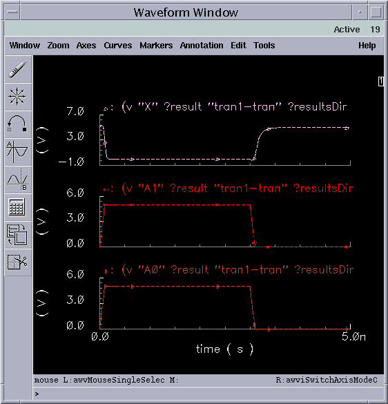
Figure2: Waveform of NOR in cadence Spectre
Then we need to generate the LVS whose tutorial is as follows: http://analog.ece.utk.edu/Cadence/LVS.htm

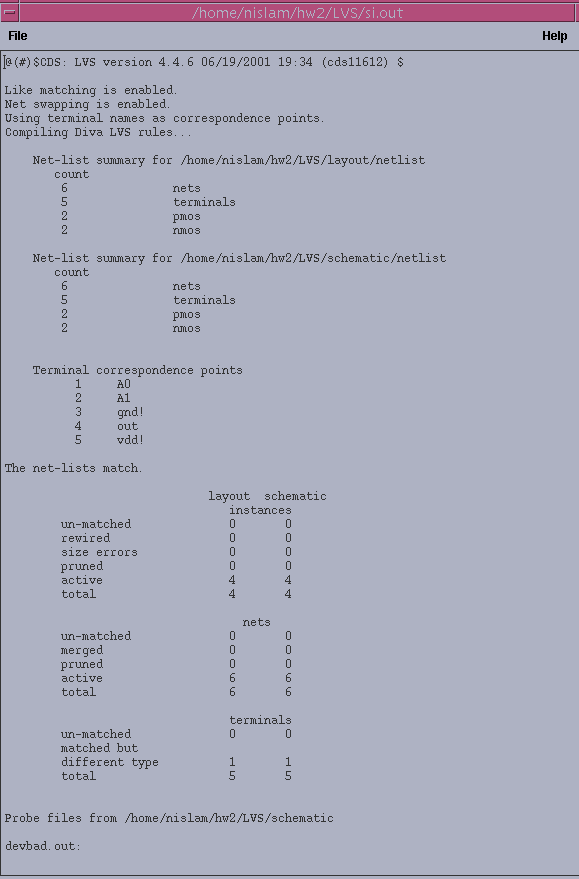
Figure3: LVS of NOR in cadence
If in the output file you get "net-lists matches", means your schematic
and layout matches perfectly.
Show TA your Simulation Waveform and Layout