By now, we have already created the schematic and have simulated our design with verilog-XL and spectre. The next step in the design process is to create the layout for the circuit. A layout is basically a drawing of the masks from which your design will be fabricated. Therefore, layout is the most critical step in the design process because it determines whether your design is finally going to be work or not.
Before we get into the layout, first we need to choose the design process we are going to use for the layout. This has in fact been specified when we attach our designs to a specific process when we create the library. In our project, the design process we are going to use is the AMI C5N process, i.e., CMOS 0.5 micron N-well process. It has 3 metal layers and the smallest feature size (generally the gate length) for this process is 0.5 micron.
The design rules we will be using for this process is the MOSIS Scalable CMOS design rules, more specifically, SCN3M_SUBM. This SCMOS design rules specifies the lambda to be 0.3 micron, i.e., the smallest feature size to be 0.6 micron, which is slightly bigger than 0.5 micron. When we use the tool to create the layout, we sometimes see some difference between the design rules from MOSIS and from our tool. If that's the case, please conform to the tool's requirement.
Now we give a tutorial on Virtuoso through creating
an example layout for the inverter cell.
- Create a layout cellview
In the library manager window, click on the File -> New -> CellView. Choose tools as Virtuoso.

Two windows appear. One is the LSW window that contains the layer information and the other is the layout editor.


- Change display options
- Draw layout shapes
- Create an inverter
- Check and save your design
- Plot your design
- Hot keys
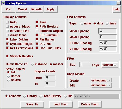
To display the layout properly, we can customize the display options. Click on Options -> Display in the layout window and the following window pops up.

In order to show the pin names, select Pin Names
in Display Controls. You can also change the Grid Controls to alter the
Minor Spacing and Major Spacing. But do not change the X Snap Spacing or
Y Snap Spacing and leave them to be half lambda. Finally you can save your
changes to the .cdsenv file.
Before we start to draw the layout, we should understand that each shape in a layout is associated with a layer. Basic layers in AMI C5N process include Nwell; active; N-select; P-select; poly; metal1,2,3; contact; via1,2; glass; pad. We will not use P-well in the AMI C5N process. There are a few layers that are used just to help layout, but does not correspond to any physical layer. For example, text layer is used to annotate the design. Cap_id, res_id and dio_id are used for layout extraction. If we want to draw a shape of a certain layer, we should click on that layer in the LSW before we draw any shape.
There are two basic types of shapes we can draw, path and polygon. Path is often used to represent "wires". Thus we often use paths to draw metal 1,2,3 and poly. This is not a restriction, but rather a common pratice. In fact, you can use path for any layer and you can also use polygon for any layer. To specify a path, click on Create -> Path in the layout window and the following windows appears.

In this window, we can specify the width for the path we draw. The default value in the width is the minimum width of the layer (metal1 in this case). We can also specify the draw style like "justification" and "end type" etc. Now we can activate the layout window and click at the point where you want the wire to start and click at every point where you want to change the direction of the wire till finally you end of the wire by double clicking at the endpoint.
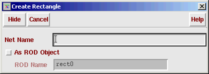
The other type of the shape is polygon. Polygons are generally used to represent the "non-wire" layers that In the layout window, click on Create -> Rectangle. The following window appears.

Now in the layout window, click on the two diagonal corners of the rectangle, we can create a rectangle.
We can also click on Create -> Polygon in the layout window to create a polygon. To draw a polygon, we should start by clicking at one of its vertices and then click at the rest of its vertices in order till we finally click at the starting vertex to form a closed shape. The following window shows a metal1 wire created by path, an nwell created by rectangle and an nwell created by polygon.

In order to know size of the polygon we just draw, we can use the ruler to measure the length and width of the shape. In the layout window, click on Window -> Create Ruler. Click at the begining and ending endpoints of the line fragments you want to measure and the distance will be shown in the layout window. In the above figure, we know that the widths of the wire and the well are all 9.9 microns. To remove the rulers, click on Window -> Clear all rulers.
A special note to contacts: In general, Contact
is of fixed size. In AMI C5N process, contacts are of fixed size 0.6 X
0.6 micron. We can either draw the contacts ourselves or add an instance
from the library.
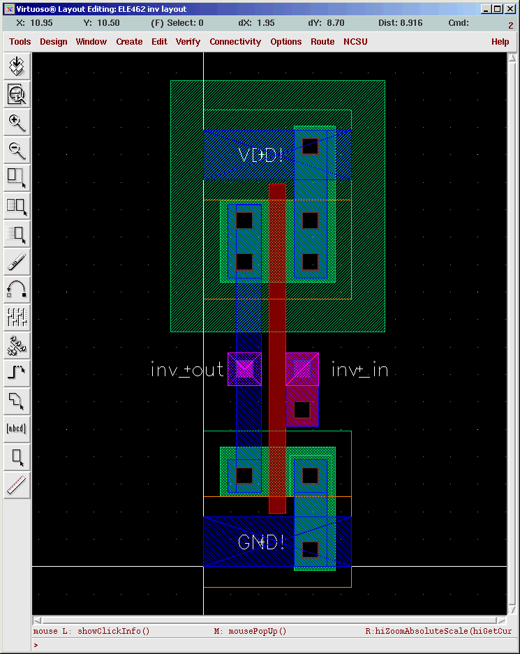
The AMI C5N process is an Nwell process, thus the substrate is p-substrate. The P-transistor should be created inside the Nwell and the N-transistor should be created outside the N-well on P-substrate directly. We will create an inverter as shown below with the following steps.

1. Create an N-well. In our case, the N-well is 7.8 X 9.15 micron
2. Create N-select and P-select. Divide the N-well into two regions. One region is P-select, it is used for the P-transistor, the other region is N-select, it is used for the N-well tub-tie. In our case, the two regions abut each other. The size for P-select is 5.4 X 3.6 micron and the size of N-select is 5.4 X 3.3 micron.
3. Create active. Note we use layer active for both P-active and N-active. If the active is within P-select, it is P-active, if it is within N-select, it is N-active. We have created a 4.2 X 3 micron active in the P-select for the P-transistor we are going to create.
4. Create the poly as the gate. In the middle of the P-active, we add the poly wire of 0.6 micron wide (i.e. 2 lambda). This creates the P-transistor.
5. Create contacts and tub tie. The poly has divided the active regions into source and drain. In order to connect the source and drain to metal, we need to create contacts. In our case, we have created two contacts for both source and drain. We have also created a contact as the N-well tub tie to connect the N-well substrate to the power source (in PMOS case, VDD). The tub tie is created in the active region (in this case N-active) to enable Ohmic contact.
6. Similarly, we can create the NMOS transistor following steps in 2-5. The only difference is that there is no well for the NMOS transistors. The NMOS transistors are created directly on top of the P-substrate.
7. Create power and ground wires. The VDD rail is generally above the the cell and the GND rail is generally below the cell. In general, the power and ground rails have a fixed spacing between them so that different cells can easily be connect in a row.
8. Connect the NMOS and PMOS transistor to form an inverter. In the layout window, use metal1 wires to connect the drain of the PMOS and NMOS together and connect the source of PMOS and NMOS to the metal wires for VDD and GND respectively.
9. Create the input and output pins. To be consistent with the schematic we created before, we use inv_in and inv_out for the input and output. In general, we use metal1 to connect intra-cell components and use metal2 and metal3 for inter-cell components. Because of this, we add a via at the output and for the metal2 wires. At the input, since metal2 cannot be connect to the poly directly, we first add a contact between metal1 to poly and then we add a via between metal2 to metal1 on top of the contact. (NOTE: AMI C5N process allow stacked contacts).
To define a pin, first select layer metal2 pin
inside the LSW window. It is an abstract layer that specifies the pin shape
only. Then click on Create -> Pin...
and the following create pin window appears.


In this window, fill in Terminal Names with inv_out and select Display Pin Name and change I/O Type to be Input. To display the pin nicely, click on Display Pin Name Option and change the height to be 0.5 micron in the "Pin Name Display" window. Create the pin now by drawing a rectangle over the via and then place the pin name.
10. Label the VDD! and GND!pins. Since the power
and ground rails all use metal1, we first select the Metal1 pin inside
LSW. Follow the steps in 9 except this time the I/O Type is jumper.
Before saving the design, we hope to make sure that the design has comform to the design rules. As careful as one might be, it is very hard for a designer to avoid all the design rule errors. To perform the design rule checking, click on Verify -> DRC... in the layout window. A pop up dialogue box will appear.

For a small circuit like an inverter, it is OK just to run the DRC in the flat mode since the running time is short. For a big layout, however, it is wise to run the DRC in a hierarchical mode. In general, hierarchical mode is faster than flat mode, especially for a large layout composed of iterative structures. However, hierarchical DRC might not be accurate in some rare cases. Thus it is a good practice to check a big circuit with hierarchical DRC first and then run a flat DRC by the end. Click on the OK button and the Diva DRC tools will be invoked the check the design and reports the errors in the CIW.

In this case, the CIW above shows that there is no error found in the DRC process. If, however, there is any error reported, the layout will be marked and CIW will indicate what kind of violations there are. You can then modify the layout and run the DRC again till there is no DRC errors.
After the cell has been checked, click on Design
-> Save... in the layout window to save your
design.
In the layout window, click on Design->Plot->Submit and the following window pops up.

Click on plot Options... and another window appears.

Modify the Plotter Name to be EPS and Paper Size
to be 8X10.5 inches and select Send Plot Only To Fileinv.ps. Click on OK
and the layout postscript file will be created under your cadence run directory.
- i: Add instances
q: Edit properties
r: Add rectangles
p: Add path
P: Add Polygon
ctrl+p: Add a pin
l: Label a wire
z: Zoom in
Z: Zoom out by 2X
ctrl+z: Zoom in by 2X
f: fit the layout in your layout window
right mouse button: repeat last command