Post layout simulation using Spectre:
1. First change the inverter schematic drawn in Lab 2.
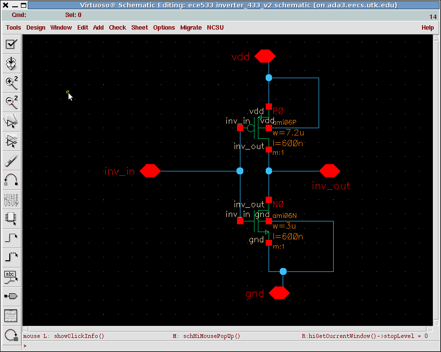
Remove the global 'vdd!' and 'gnd!' pins and add them as
'inputoutput' pins. See the figure below.
Please do not use '!' mark in any of the pins.
2. Create the symbol again. In the inverter schematic view click
Design > Create Cellview > From Cellview > OK > modify > YES
You will get a modified symbol. Arrange it according to the following figure.

3. Change the 'inverter_test' schematic view accordingly.

4. Copy the layout drawn in Lab 4 to Lab 2. Make sure that all the pins in the layout and schematic are 'exactly' same.
check the spelling (upper/lower case), direction of the pin, etc.
Open the layout and run DRC. Verify > DRC
5. If it is DRC clean then run Extract. Verify > Extract
In the extractor window > switch names > click 'Set Switches' button and select 'Extract_parasitic_caps' > OK > OK

Open the extracted view. press 'shift+F'. Make sure that all the PMOS and NMOS are exactly same size as the schematic.
6. Run LVS (Layout vs. Schematic) from layout or extracted view. Click Verify>LVS
click Form Contents > OK
In Artist LVS window select the views of schematic and extracted (by default they are selected) of which you want to run LVS.

click Run and wait. If you get the success window then click OK. In Artist LVS window click Output.
If you do not get the success window then try to find out the problems in
the ICFB window. Problem could be in DRC, saving the last view, etc.
If you have succeeded it would open 'si.out' window and say 'The net-lists match'....... Hooray !!
Otherwise it would say, 'The net-lists failed to match'. Then try to find out the errors from the bottom of the si.out window.

Post layout simulation:
In lab2 library, You have one cell named 'inverter'. In 'inverter' you should have 4 views - schematic, symbol, layout, extracted.
And your LVS is matched.
Now we are ready to perform post layout simulation.
Open the 'inverter_test' schematic. and Run the simulation tool virtuoso ADE from Tools > Analog Environment >
Follow all the steps from 'Simulation' given in the
spectre
simulation instruction
In virutoso ADE window click Setup > Environment > Switch view list > rewrite 'schematic' to 'extracted'

Create the netlist again. Virtuso ADE window Simulation > netlist > Recreate
Make sure that the view name is extracted in the recreated netlist.

Now Run the simulation.
you can save the state as extracted or any name you like........
For simulating next labs:
Make sure you have all 4 views of same cell, (say 'X')- schematic, symbol,
layout and extracted.
Make sure that layout is DRC clean and LVS is matched.
Create a cell named X_test, which would have all the input sources.
Run simulation from X_test schematic and save the state. For post layout
simulation follow the steps below:
Follow all the steps from 'Simulation' given in the
spectre
simulation instruction
In virutoso ADE window click Setup > Environment > Switch view list > rewrite 'schematic' to 'extracted'
Create the netlist again. Virtuso ADE window Simulation > netlist > Recreate
Make sure that the view name is extracted in the recreated netlist.
Now Run the simulation.
Congratulations !!