
Power Delivery PCB
Motivation
One of my research assignments while in the TENNLab Neuromorphic Research Group, GRANT, was a robot that autonomously roamed around a room to find a target while avoiding obstacles in its path. This platform required several external sensors and interface devices that drew a decent amount of current (2-3 A) at variable voltage levels. One of the main problems that kept creeping up on us was properly delivering power to these devices without several points of failure and random voltage drops that caused strange USB behavior. To solve these issues, I attempted to create this Power Delivery PCB to be a general purpose robotics power delivery board that could handle high current (up to 5A) and provide a constant regulated voltage output with a wide range of acceptable input voltages.
Design Objectives
My objectives with this power delivery board included the following:
- Support multiple input options for power
- Allow for hotswapping input power with prioritization
- Support up to 5A of continuous current
- Integrate undervoltage and overvoltage protection into the PCB
- Include a fuse for overcurrent protection
- Able to step voltage up or down for a wide range of input voltages
- Have multiple output options for power
Specifications
The final specifications for the board are detailed in the following table:
| Item | Spec |
|---|---|
| PCB Size | 45mm x 100mm |
| Layers | 2-4 |
| Input Voltage | 3-16V |
| Output Voltage | 0.7-18V |
| Max Current | 5A |
| Input Sources | 3 |
| Output Sources | 3 |
| Protections | UV, OV, and OC |
Design Attempt 1
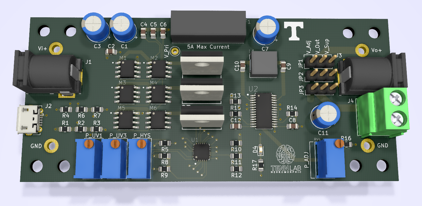
Originally, two main chips were chosen to achieve the functionality that I desired. This was the LTC4417 PowerPath Controller and the LTC3119 Buck-Boost DC-DC Converter.
The LTC4417 has integrated independent undervoltage and overvoltage protection for three different input sources as well as the added benefit of hot swapping capability for those three inputs. The hot swapping works by assigning a priority to each of the three inputs to the chip. If multiple inputs have valid power, i.e. are within the voltage limits set by UV and OV, the output is fed by the input with higher priority. The chip accomplishes this by controlling the path from the inputs to the output with high current FDS4685 FETs.
The LTC3119 is a wide input voltage (2.5-18 V) buck-boost regulator that has a maximum boost current of 3 A and a maximum buck current of 5 A. The output voltage is controlled by a potentiometer that allows the chip to adjust the output voltage between 0.7 V and 18 V. The buck-boost capability means that it is able to keep a consistent output voltage independent of the input voltage so long as the input voltage is within the wide valid input range.
Schematic
Here is a PDF of the schematic created using KiCAD:
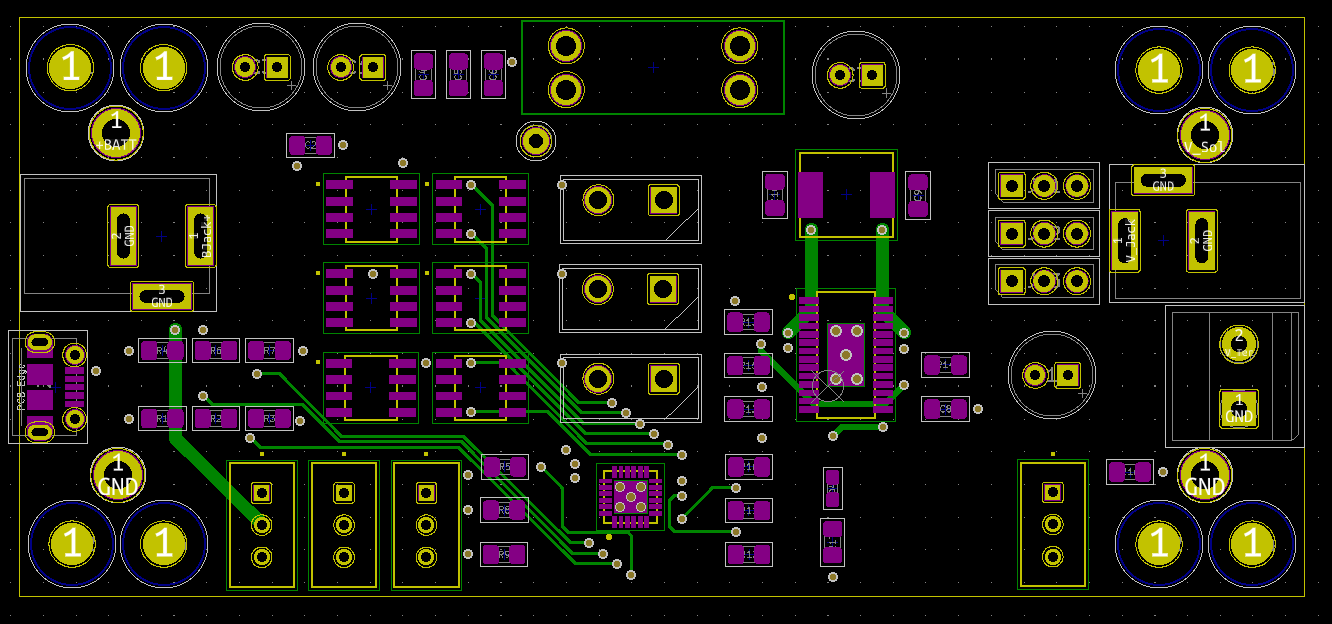
PCB Layout
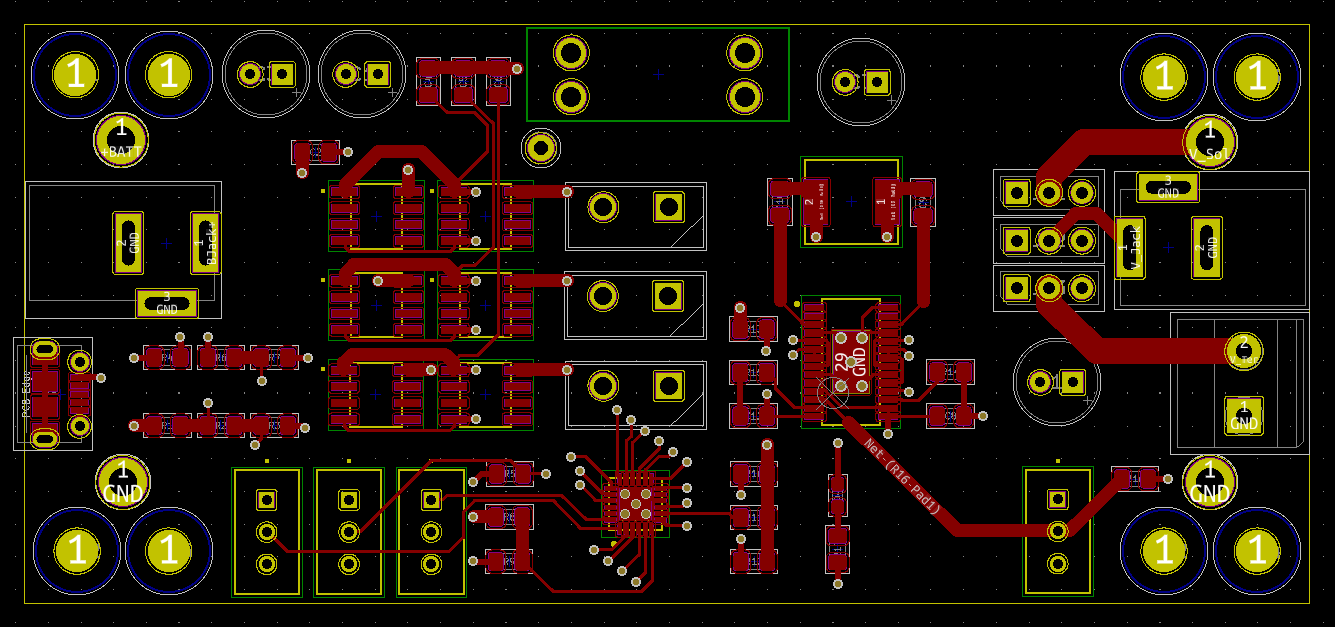
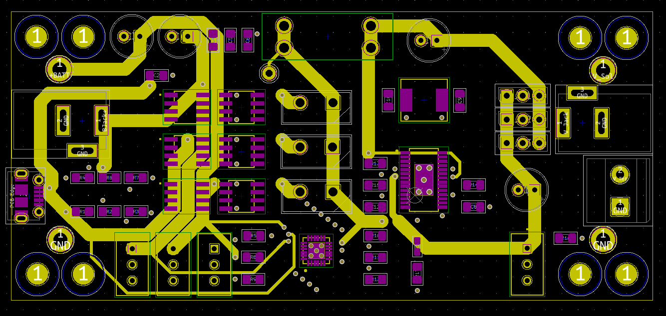
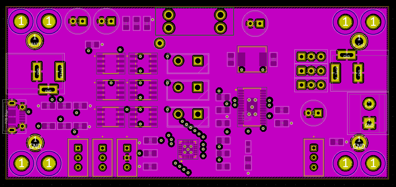
Here are images of each PCB layer layout, all designed with KiCAD:
Front Layer
Power Layer
Ground Layer
Bottom Layer
First Attempt Results
The first design attempt had several flaws. The first, most severe flaw was that the LTC3119 chip was not working as intended. Even though the chip is rated for currents between three and five amps, regulation of output voltage would fail at even the lightest of loads.
The other flaws were simply bad PCB design practices on part: bad choices for capacitors, nonideal placements, nonideal trace widths, etc. These things could have contributed to the failure of the LTC3119, but it is hard to determine exactly why it was failing.
Second Design Attempt
Please stay tuned for an update on this!
