Introduction
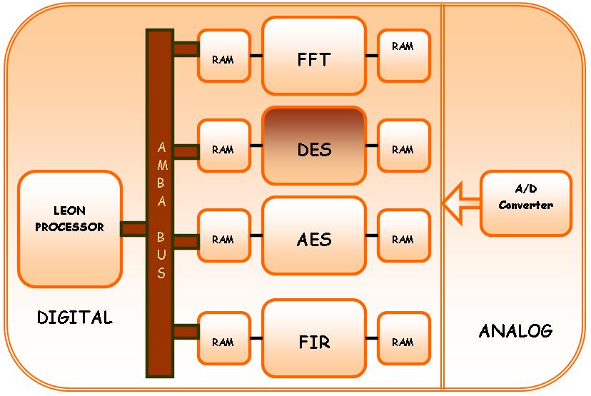
System on a Chip (SoC) is an IC designed by switching together multiple stand-alone VLSI designs to provide full functionality for an application. The System on a chip design concept emphasizes the use of models called cores also called intellectual property (IP) block or virtual components or macros. The predesigned cores are generally available in either synthesizable high-level description language (HDL) form such as Verilog/VHDL (Soft Cores/Firm Cores), or optimized transistor-level layout such as GDSII (Hard Cores). The following figure shows the general architecture of our system on a chip. The figure shows the highlighted DES IP block used in our project. The Leon Processor and all the IP blocks - Fast Fourier Transform (FFT), Data Encryption Standard (DES), Advanced Encryption Standard (AES) and the Finite Impulse Response (FIR) are linked through the Advanced Microcontroller Bus Architecture (AMBA).

Figure: General Architecture of our System on a Chip
The objective of our project is as follows: To pass the input data stored in the Input RAM to the DES block. The DES block would perform the encryption operation on the data and store the ciphered text back in the Output RAM. The design entry used the HDL description (VHDL) of Asynchronous Dual Port RAM and the Data Encryption standard (DES) IP blocks. The logic simulation was performed for the RTL description to ensure the functionality of our design. The HDL netlist was then synthesized using Synopsys Design Compiler tools to obtain the gate level netlist. The gate level simulation was performed using back-annotated delays in the Verilog/VHDL netlist to ensure functionality and timing. The place and route was done using Silicon Ensemble and then exported to Cadence Virtuoso environment. The Design Rule Check and Layout versus Schematics (LVS) checks were done to ensure that the design was free from design rule violations and it did match with the schematic corresponding to our gate level netlist.