|
User |
Guide |
|
| |
| |
|
Working
of the System. |
|
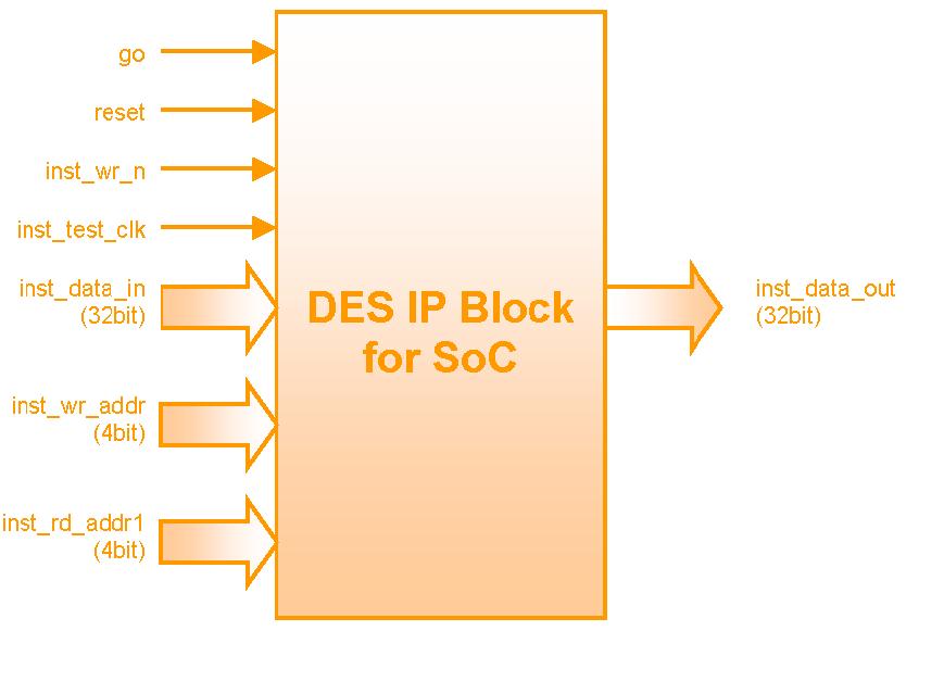
As
already explained the IP block consists of an Input RAM , Output RAM
and the DES. The data to be encrypted is written into the input RAM
and when the ‘go’ signal is made high the data in the Input RAM is
encrypted and written to the Output RAM.
|
|
|
Description
of the signals
|
|
inst_test_clk
– Clock Signal to all the blocks , 10 MHz
|
|
A
clock of 5MHz is to be supplied to this pin
|
|
|
|
inst_wr_addr
(4 bit , expandable to 8bit) – Input RAM Write Address
|
|
This
is used to supply the write address to the input RAM
|
|
|
|
inst_data_in
(32bit)
– Input
Data Bus
|
|
This
is used to supply the data to the input RAM.
|
|
|
|
|
|
go
‘Active High’ – Begins Encryption
|
|
This
signal should be made high after the data is completely entered into the
Input RAM . This signal starts the encryption process by reading the data
from the Input RAM and feeding it to the DES. |
|
|
|
reset
‘Active High’ – Resets all the counters and address pointers to
initial values. |
|
This
signal should be made ‘high’ for 100ns and then back ‘low’ before
writing the data into the Input RAM. |
|
|
|
inst_wr_n
– Write
Enable |
|
This
signal is used to write the data present on the data bus (inst_data_in) to
the address location on the address bus (inst_wr_addr) once the data and
the address are available on the respective buses . |
|
|
|
inst_rd_addr1
(4 bit , expandable to 8bit)
– Output
RAM Read Address |
|
This
is used to supply the address to read the stored encrypted data from the
output RAM.
|
|
|
|
inst_data_out1(32
bit)
– Output
data bus |
|
This
is used to read the encrypted data from the output RAM specified by the
address location present on the address bus (inst_rd_addr1).
|
|
|
|
Expanding
the depth of the RAM
|
|
| For
Testing of this block the depth of this RAM was fixed at 16 but is
expandable to 256. Accordingly the bus width will have to be
expanded to 8 bit. |
| For
this the following changes will have to be done. |
| In
the design ware RAM block (DW_ram_r_w_a_dff_inst.vhd) change the
‘inst_depth’ to 256 . Accordingly the address bus with at all
places will have to be changed to 8 bits.
|
| The
data count is currently set to 2 in the controller.v file . Change
this to (depth/4). |
| |
From
writing the data into the Input Ram to Obtaining Output
|
| This
Encryption block excrypts a 64 bit plain text with a 64 bit
key input . Since the SoC system bus was fixed at 32bit wide we have
split the plain text and the key to two words of 32bits . The first
location of the Input RAM is the LSB of the key and the second
location is the MSB . The third location in the RAM is the LSB of
the plain text and the fourth location is the MSB of the plain text.
This order must be maintained for all the input data. |
| ->
Reset should be made high and then low again |
| ->
Place the address in the address bus of the Input RAM at the rising
edge of the clock |
| ->
Place the data in the data bus of the Input RAM at the next rising
edge |
| ->
Make the inst_wr_n high the next clock for one clock cycle. |
| This
process must be repeated for each data.
|
| ->
After the data is written to the RAM the ‘go” signal must be
made high. |
|
The
64 bit encrypted data is split into two words of 32 bit width. The
LSB is written in address location ‘0000’ and the MSB is written
in address location ‘0001’. This format continues for all
encrypted data. |
| ->
To read the encrypted data the address must be placed on the
(inst_rd_addr1) Output RAM address bus . |
|
|