This module was developed Adam Miller at the electrical engineering department at the University of Tennessee.
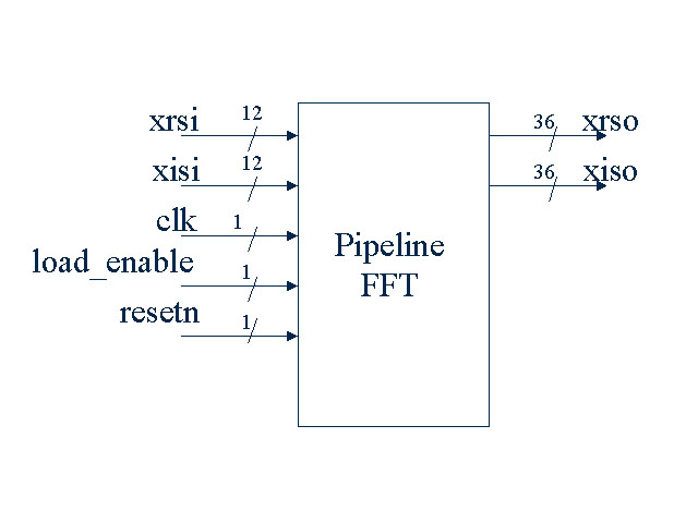
Inputs/Outputs:
xrsi : Data Input, Real part of complex integer values, 12-bit wide
xisi : Data Input, Imaginary part of complex integer values, 12-bit wide
xrso : Data Output, Real part of complex integer values, 36-bit wide
xiso : Data Output,Imaginary part of complex integer values, 36-bit wide
clk : Control Inputl, Standard Logic
reset_n : Control Input, Standard Logic
load_enable : Control Input, Standard Logic
Description:
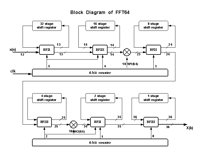
The 64-sample pipeline FFT is based on the Radix-22 Single-path delay Feedback architecture.
This architecture processes the input data in the natural order and gives the output in bit-reversed order.
Input data is received one sample per clock cycle and output data is generated one sample per clock cycle.
Data is accepted by the FFT for 64 clock cycles and it starts producing the output at the 64th clock cycle. The next frame of transform can be computed without pausing due to the pipelined processing of each stage. The data for each point are synchronized with the rising edge of the clock when the load_enable is active high. The data is then fed into the FFT core and the output data in bit-reversed order is produced after the 63rd clock cycle. The next 64-sample data frame can follow the first frame continuously.
Timing and Operation:
Pre-synthesis simulation:
FFT starts accepting the input data after the load_enable goes high. This input data can be supplied from
a textfile or a RAM. Two 12-bit vectors are sent to the FFT for 64 clock cycles. After the 63rd
clock cycle the FFT starts producing two output vectors, each of 36 bits width, for every clock cycle.


The output can be written to a textfile or to an output RAM. In the case of FFT stand alone module, the input is
read from a textfile and the output produced is written to another textfile.


Post-layout simulations:
After the presynthesis simulations, the FFT module has been synthesized using Synopsys Design Compiler.
The netlist file, fft.v in this case, is then imported into Silicon Ensemble along with the tsmc18 general constraint
file and the tsmc18 6-metal layer layout exchange format file for generating the physical layout.
After the placement and routing, the .dspf and .def files are exported from Silicon Ensemble. These files are
used to generate the .sdf file which is used for the post-layout simulation.


In the post-layout simulation, the output in each cycle takes some time before reaching a constant value. This can be noticed
at the thick green lines before each output cycle.


Layouts:
FFT targeted to Xilinx Virtex 1000e:


