Next: Source Code and Conclusions
Previous: FFT
RAM-FFT-RAM Modules
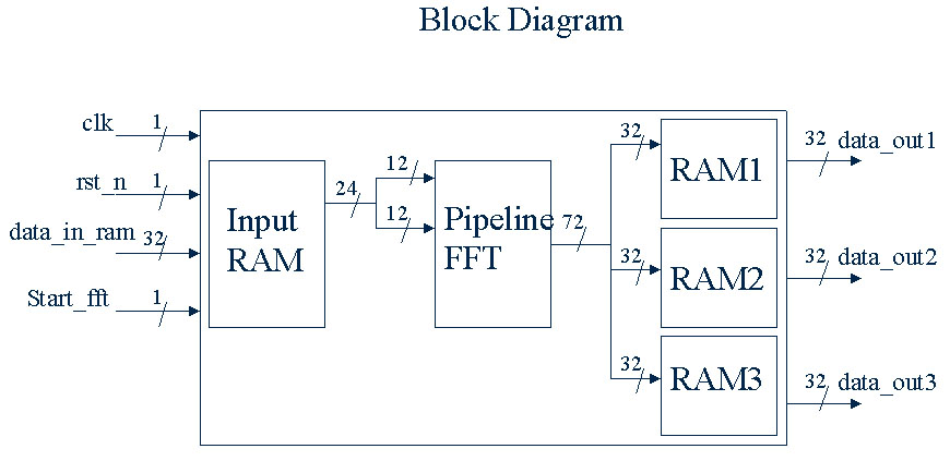 Figure 2.0 Block Diagram of RAM-FFT-RAM Module.
This module consists of an addition to the FFT standalone module. Input data to the FFT is read from the input
RAM and also output data is written to the output RAMs. The depth of each RAM is 64 and the data width
of each RAM is 32-bit wide.
Inputs/Outputs:
data_in_ram: Data Input, Complex integer values, 32-bit wide
data_out1 : Data Output, Complex integer values, 32-bit wide
data_out2 : Data Output, Complex integer values, 32-bit wide
data_out3 : Data Output, Complex integer values, 32-bit wide
clk : Control Input, Standard Logic
rst_n : Control Input, Standard Logic
start_fft : Control Input, Standard Logic
Description:
The input to this module is data_in_ram, and it takes in a 32-bit vector according to the AHB Bus width.
The RAM stores 64 32-bit vectors and outputs 64 24-bit vectors to the FFT module when start_fft signal becomes high at
the rising edge of the clock. The FFT reads the data for 64 clock cycles and starts producing the output
after the 63rd cycle. The 72-bit output vector from the FFT is divided into two 32-bit vectors and one
8-bit vector. The first 32-bit vector is written to the Output RAM1 starting from the zero location.
The second 32-bit vector is written to the Output RAM2 starting at the zero location. A 24-bit vector of zeros
is then appended to the last 8-bit vector. The resulting 32-bit vector is written to the Output RAM3 starting at the
zero location. The same procedure applies to all the output vectors from the FFT.
Three output RAMs are required to store the output of the FFT because each RAM is only 32-bit wide and the recommended
depth is 64. Data can be read from the output RAMs at any time according to the users' request.
When the user requests the data from the output RAMs at the same time as it is being written, the output will be seen
after one clock cycle.
Timing and Operation:
Pre-synthesis simulation:
Data is written into the input RAM one vector per clock cycle when inst_rst_n becomes high. The write address
(inst_wr_addr) of the input RAM is incremented every clock cycle as seen in Figure 2.1 below.

Figure 2.1 Pre-synthesis Simulation of RAM-FFT-RAM Module (Part 1).

Figure 2.2 Pre-synthesis Simulation of RAM-FFT-RAM Module (Part 2). The FFT starts
reading the data into xrsi and xisi from the input RAM when the load_enable signal becomes high. At this time
the read address (inst_rd_addr) of the input RAM starts incrementing at each clock cycle, supplying data to the FFT.
Refer to the figure above.

Figure 2.3 Pre-synthesis Simulation of RAM-FFT-RAM Module. FFT starts generating the
output after 63 cycles of input data. Refer to the signal inst_rd_addr in the figure above.
The outputs xrso and xiso are passed to the three output RAMs. The write addresses (inst_wr_addr) start
incrementing from this time. From the figure above it can be seen that the first 32 bits of the output are
sent to the Output RAM1. The second 32 bits are sent to the Output RAM2 and the remaining 8 bits are sent to
the Output RAM3.

Figure 2.4 Pre-synthesis Simulation of RAM-FFT-RAM Module. This figure shows the full
funcionality of the RAM-FFT-RAM module and the point where the input to the FFT starts.

Figure 2.5 Pre-synthesis Simulation of RAM-FFT-RAM Module. This figure shows the full
funcionality of the RAM-FFT-RAM module and the point where the output from the FFT starts.
Post-layout simulations:
After the presynthesis simulations, the RAM-FFT-RAM module has been synthesized using Synopsys Design Compiler.
The netlist file, ramfftram4a.v in this case, is then imported into Silicon Ensemble along with the tsmc18 general constraint
file and the tsmc18 6-metal layer layout exchange format file for generating the physical layout.
After the placement and routing, the .dspf and .def files are exported from Silicon Ensemble. These files are
used to generate the .sdf file which is used for the post-layout simulation.

Figure 2.6 Post-layout Simulation of RAM-FFT-RAM Module (Part 1).
Data is written into the input RAM one vector per clock cycle when inst_rst_n becomes high. The write address
(inst_wr_addr) of the input RAM is incremented every clock cycle as seen in Figure 2.6.

Figure 2.7 Post-layout Simulation of RAM-FFT-RAM Module (Part 2).
The FFT starts reading the data into xrsi and xisi from the input RAM when the load_enable signal becomes high. At this time
the read address (inst_rd_addr) of the input RAM starts incrementing at each clock cycle, supplying data to the FFT.
Refer to the figure above.

Figure 2.8 Post-Layout Simulation of RAM-FFT-RAM Module.
FFT starts generating the
output after 63 cycles of input data. Refer to the signal inst_rd_addr in the figure above.
The outputs xrso and xiso are passed to the three output RAMs. The write addresses of the three output RAMs (inst_wr_addr)
start incrementing from this time. From the figure above it can be seen that the first 32 bits of the output are
sent to the Output RAM1. The second 32 bits are sent to the Output RAM2 and the remaining 8 bits are sent to
the Output RAM3.

Figure 2.9 Post-Layout of RAM-FFT-RAM Module.
The read address (inst_rd_addr) of the output RAMs is given at the same time as the write address for all the 64 output vectors.
The data from the output RAMs therefore cannot be seen until the read address starts over again.

Figure 2.10 Post-Layout Simulation of RAM-FFT-RAM Module.
This figure shows the full funcionality of the RAM-FFT-RAM module and the point where the input to the FFT starts.

Figure 2.11 Post-Layout Simulation of RAM-FFT-RAM Module.
This figure shows the full funcionality of the RAM-FFT-RAM module and the point where the output from the FFT starts.

Figure 2.12 Layout generated in Silicon Ensemble

Figure 2.13 Layout in Virtuoso
The .def file produced in Silicon ensemble is imported into Cadence Virtuoso to generate the above layout.