
Schematic Composer
At this point, you have created a library
to store your design and can start the design process. For a full custom
design, the process begins by creating a schematic. Then we simulate this
design to verify the correctness of its functionality and explore its switching
behavior in order to optimize the performance. Only after this is done,
we will start the layout of the design.
- Create a new schematic
- Add an instance
- Set Properties
- Connect the instances with wires
- Create pins and labels
- Check and save the designs
In your Library Manager window, click on the File->New->Cellview. A pop-up dialogue box appears. Click on the library name button and select "ELE462". Click on the Tool button to select "Composer-Schematic". The View Name will automatically change to "schematic". Enter the name of the cell you wish to design in Cell Name. For the tutorial case, we design an inverter.

This will pop-up an empty Schematic Creation Window.
We will talk about how to create an inverter in this schematic window in
the following steps. We will start by adding an instance of NMOS and an
instance of PMOS.
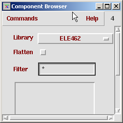
To place an instance, e.g. an NMOS device, in your schematic, activate the schematic window, then click on Add->Instance (or type i). The "Add instance" dialogue box appears together with the "component Browser" dialogue box. (In case the "Component Browser" does not appear, click on browse in the "Add Instance" dialogue box to start it.)

In "Component Browser" window, Click on Library and choose NCSU_Analog_Parts. Click on N_Transistors and choose nmos4 as your NMOS device. To place the instance, activate the schematic window and click the left mouse button to put the instance at the place desired.
Note in Cadence schematic composers and layout
editors, a command will not terminate unless the user cancels it or the
user starts a new command. In this case, you can see another instance is
ready to be placed right after you placed the first instance. To terminate
the current operation (which is "add instance" in this case), press ESC
key on the keyboard. In fact, you can always cancel the current operation
in schematic or layout editors by pressing ESC key.
To set the property of the instance that you just placed or any object in your schematic or layout design, select the object by clicking on it and then go to "Edit->properties->Object..." (or by typing q). An object properties editing form will pop up.
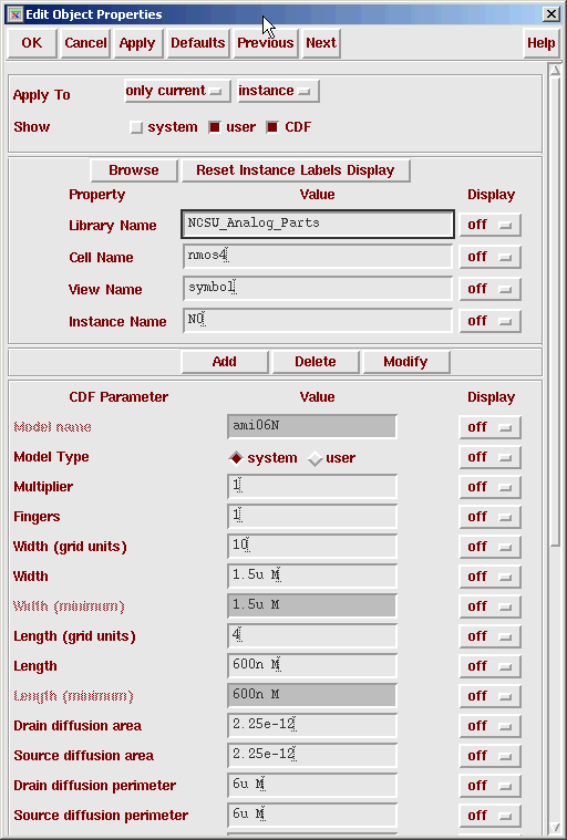
Change the width or length of the gate to the
desired value. In this case, we use the default value. Following the same
techniques, we can add an instance of PMOS transistor.
To connect the PMOS and NMOS devices or any electrically connected devices, click on Add->Wire(narrow) in the schematic window (or type w). Click at the terminal where the wire starts and click at the terminal where the wire ends, a wire will be automatically added. If you are not satisfied with the automatic wiring, you can remove the wire and reroute it manually. This time, instead of clicking at the terminal where the wire ends directly, you can click the left mouse button whenever you want to change the wire direction.
If you want to stop the wire somewhere instead
of connecting it to a terminal, double click your left mouse button and
a dangling wire is created. In general dangling wire should be avoided,
however, in some cases (like you want to label this wire or add a pin to
this wire), a dangling wire makes sense.
For any cell, we have to specify its input/output behavior. We can achieve this through adding the pins for its input and output. For some global wires (like VDD and GND), we can simplify the I/O of the schematic by adding a label to each one of them.
Click on "Add->Pin..." (or type p) in the schematic window, the following dialogue box would appear.

For an input pin, Choose the Direction to be input. Specify the Pin Names (inv_in in the example). Activate the schematic window and click on the left mouse to put the pin. Similarly we can put an output pin (inv_out in the example) to the output of the cell.
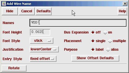
Adding labels to the wires is similar to adding pins. Click on "Add->Wire Name..." (or type l) in the schematic window, the following dialogue box would appear. You can specify a name for each wire, but we generally only add labels for those global wires like "VDD" or "GND". In order to denote a global wire name, you have to add a "!" after the wire name (VDD! in our example).
After the design has been completed, click on "Design->Check and Save" to check and save your designs. Check the CIW window to see if there is any errors in your designs. The following image shows the completed design of inverter.

- Hot keys
- i: Add instances
q: Edit properties
w: Add wires
p: Add a pin
l: Label a wire
z: Zoom in
Z: Zoom out by 2X
f: fit the schematic in your schematic window
right mouse button: repeat last command