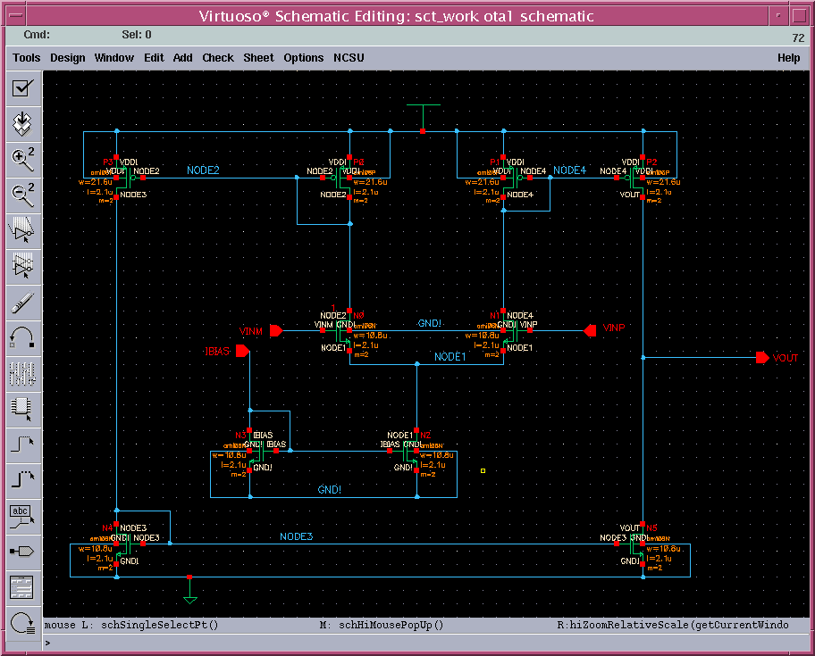
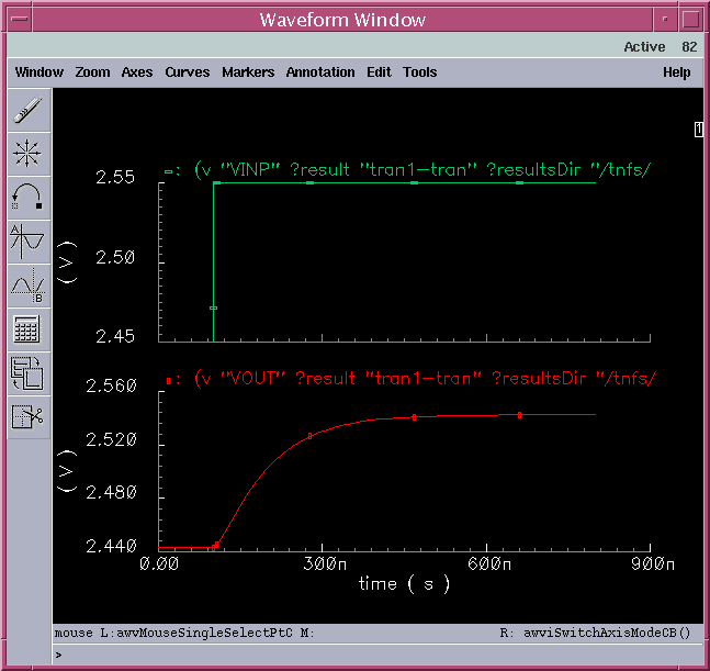


Introduction: The purpose of this homework assignment is to introduce introduce important concepts pertaining to the layout of analog integrated circuits. The basic topics that will be covered are: 1. Why analog integrated circuits? 2. Important techniques used in the layout of analog integrated circuits. 3. Analog design flow and tutorial highlighting important analog layout techniques. (For questions please e-mail sterry2@utk.edu) =================================================================================== 1. Why analog integrated circuits? Considering the great push in the electronics industry towards implementing signal processing functions in the digital domain, a common question is "Why do we study the design of analog integrated circuits?" The most straightforward answer to this question is that the real world is in fact analog (i.e. signals vary continuously in time and amplitude), therefore any system with inputs and/or outputs that interface to the real world must contain analog signal processing functions. Some common examples of everyday systems which have analog interfaces are: 1. RF transceiver in a cell phone 2. Remote sensors and monitoring (e.g. temperature monitors) 3. High Speed optical interface circuits It is important to note that that very few modern integrated circuits and systems are purely analog. In most cases a circuit design team will include digital and analog systems on a single chip, thus the complete system would be classified as "mixed-signal." It is predicted that by 2005 60% of all circuit designs will be classified as mixed-signal. =================================================================================== 2. Important techniques used in the layout of analog integrated circuits. Introduction: The layout of analog integrated circuits is often driven by several issues that are generally not important in digital circuits. Therefore it is important for the layout engineer and designer to be aware of these issues. Important Analog Issues: A. Matching of Devices: Matching of individual devices is of paramount concern in analog circuit design. Infact almost all of the 'analog layout techniques' are actually methods for improving matching between different devices on a chip. Matching is important because most analog circuit designs use a ratio based design technique(e.g. current mirrors). Some common techniques that help improve device mathcing are MULTI-GATE FINGER LAYOUT and COMMON-CENTROID LAYOUT. B. Noise: Noise is important in all analog circuits because it limits dynamic range. In general there are two types of noise, random noise and environmental noise. Random noise refers to noise generated by resistors and active devices in an integrated circuit; environmental noise refers to unwanted signals that are generated by humans. Two common examples of environmental noise are switching of digital circuits and 60 Hz 'hum'. In general, random noise is dealt with at the circuit design level. However the are some layout techniques which can help to reduce random noise. MULTI-GATE FINGER LAYOUT reduces the gate resistance of the poly-silicon and the neutral body region, which are both random noise sources. Generous use of SUBSTRATE PLUGS will help to reduce the resistance of the neutral body region, and thus will minimize the noise contributed by this resistance. Enivironmental noise is also dealt with at the circuit level. One common design technique used to minimize the effects of environmental noise is to employ a 'fully-differential' circuit design, since environmental noise generally appears as a common-mode signal. However SUBSTRATE PLUGGING is also very useful for reducing 'substrate noise', which is a particularly troublesome form of environmental noise encountered in highly integrated mixed-signal systems and Systems-On-a-Chip (SOC). Substrate noise occurs when a large amount digital circuits are present on a chip. The switching of a large number of circuits discharges large dynamic currents to the substrate, which cause the substrate voltage to 'bounce'. The modulation of the substrate voltage can then couple into analog circuits via the body effect or parasitic capacitances. SUBSTRATE PLUGGING minimizes substrate noise because it provides a low impedance path to ground for the noise current. ***Note: Issues that are important in digital circuits are still important in analog layout. Foremost among these is parasitic aware layout. It is important to minimize series resistance in digital circuits because it slows switching speed. Series resistance also slows analog circuits, plus it introduces unwanted noise. Parasitic capacitance is avoided in digital circuits because it slows switching speed and/or increases dynamic power dissipation. Stray capacitance has the same effect in analog circuits (bias current must be increased to maintain bandwidth and/or slew rate when extra load capacitance is present) plus it can lead to instability in high gain feedback systems. Definition of Bold Terms: A. MULTI-GATE FINGER LAYOUT refers to implementing a single, wide transistor as several narrow transistors in parallel. This minimizes the gate resistance and it also makes it easier to match the transistor with other devices. When referring to a multiple gate finger device one usually uses the term 'M-factor' to refer to the number of gate fingers. Therefore an M=4 device has 4 gate fingers. Note: When trying to ratio two or more devices you should always use the same unit transistor size for each device and then include multiple gate fingers to achieve the desired ratio. For instance, a current mirror containing a 10/2 and 5/2 device is NOT a perfect ratio of two because of oxide encroachment. However a 5/2 M=2 device and a 5/2 M=1 device is a perfect ratio of two. B. COMMON-CENTROID LAYOUT refers to a layout style in which a set of devices has a common center point. This is used to minimize the effect of linear process gradients (e.g. oxide thickness) in a circuit. Example: Consider that a transistor 'A' has 'M' fingers and can be represented by 'M' instances of the letter 'A'. For example 'AAAA' represents a transistor 'A' that has 4 fingers. Now consider the layout of two transistors, 'A' and 'B'. One structure is: AABB The problem with this structure is that the transistor 'A' will have a different oxide capacitance (which affects transconductance, Ft) than 'B' because of oxide gradients. For instance, if the oxide thickness at the center of the structure is Tox, and there is an oxide gradient DEL, the average oxide thickness for 'A' and 'B' is Tox(A, average) = [Tox - 2DEL]/2 + [Tox - DEL]/2 = Tox - 3DEL/2 Tox(B, average) = [Tox + 2DEL]/2 + [Tox + DEL]/2 = Tox + 3DEL/2 Now consider the following layout: ABBA The average oxide thickness will now be: Tox(A, average) = [Tox - 2DEL]/2 + [Tox + 2DEL]/2 = Tox Tox(B, average) = [Tox - DEL]/2 + [Tox + DEL]/2 = Tox. Many other common centroid layout structures are possible: ABCCBA, ABBBBA, ... Also in two dimensions: AB BA OR ABAB BABA ABAB BABA C. SUBSTRATE PLUGGING simply refers to making an ohmic contact to the substrate. This technique is used in digital circuits to minimize latch-up. In analog circuits it is used to minimize latch-up and for the reasons discussed above. For more information please see: [3] [4] [5] =================================================================================== 3. Analog design flow and tutorial highlighting important analog layout techniques. Now the layout of an analog circuit will be presented with an emphasis on the concepts presented in Section 2. The design flow is the same as for digital circuits, except we do not Verilog. Therefore the steps are: A. Enter Schematic B. Pre-layout Simulation Using Spectre C. Custom Layout Using Virtuoso D. Extraction and LVS E. Post-Layout Simulation Using Spectre A. Schematic The circuit presented in this tutorial is the so-called simple operational transconductance amplifier (OTA). The schematic is shown here.Figure 1. Complete OTA Schematic You can also download a PDF version here. Another pdf version. Note that 'L' has been chosen much larger than the minimum. This is done to improve matching and increase gain. Also note that all devices have been specified as having two gate fingers. To set this parameter change the 'Multiplier' field in the device properties to two. B. Pre-Layout Simulation: First generate a run file, 'si.inp', as usual. You will have to add several statements to the run file so that we can simulate the 'small-signal step response.' My run file is here. Next simulate the circuit and bring up the spectre waveform tool. Plot the signals 'VOUT' and 'VINP'. Here is my result:
Figure 2. Pre-Layout Simulation A PDF version is available here. C. Custom Layout: C1. Layout of 1-Gate Finger I started with the layout of the N2, N3 current mirror. Here is the layout of one transistor finger. It measures 10.8um by 2.1um.
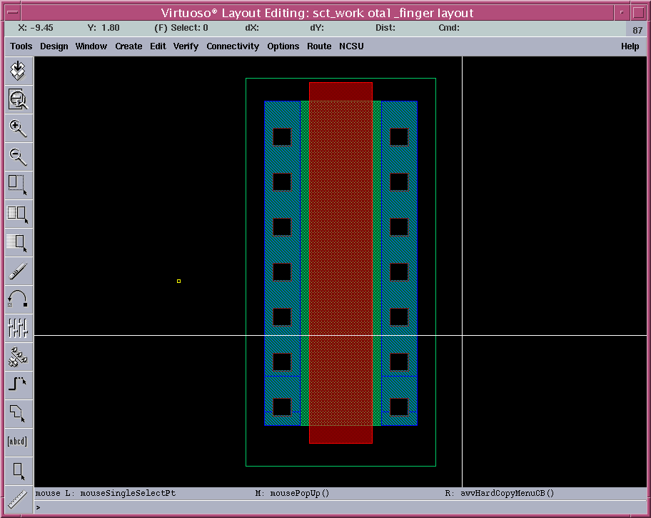
Figure 3. One NMOS Transistor Finger Note: We don't have to worry about substrate contacts yet. C2. Combine 4-Gate Fingers for N2, N3 current mirror Next array 4 gate fingers to create the shared source/drain structure. This will allow us to implement an 'ABBA' common centroid.
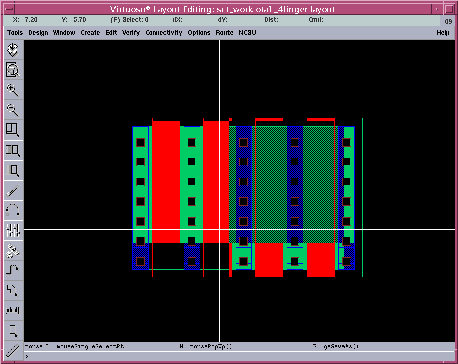
Figure 4. Layout of all gate fingers for N2,N3 Mirror. C3. Add drain and gate routing for N2, N3 current mirror. Here is N2,N3 with the drain and gate routing. Note the shared source/drain structure. The sources are floating right now. Once the body ties are included the sources will be routed to the body ties.
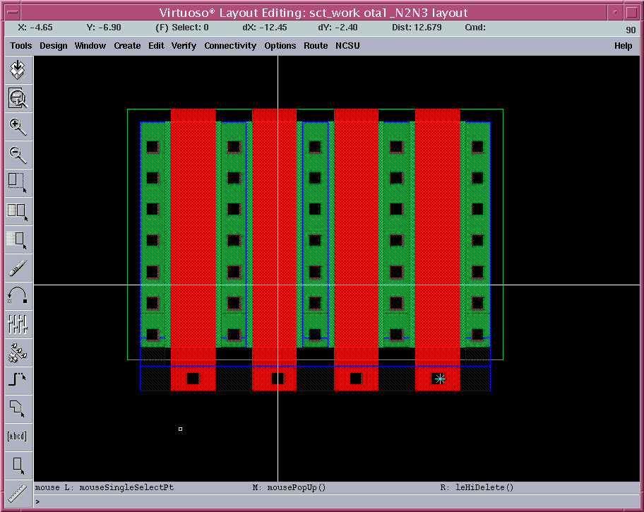
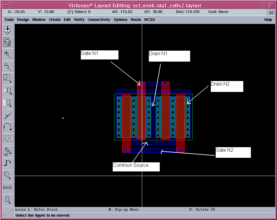
Figure 5. Layout of N2,N3 with routing.
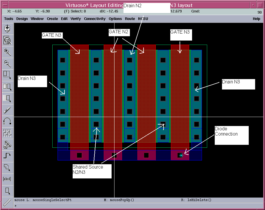
Figure 6. Layout of N2,N3 with routing and annotation. C4. Add N4, N5 to complete NMOS current mirrors. Next I added N4, N5 using the same 'ABBA' structure. They are placed outside of the N4,N5 mirror, similar to the schematic. Note that since all there structures are very similar, you can rely heavily on copy/paste.
Figure 7. Layout of N2,N3,N4,N5.
Figure 8. Layout of N2,N3,N4,N5 with annotation. C5. Layout of NMOS Differential Pair The NMOS current mirrors are complete for now, next is the differential pair N0, N1. Again I used the 'ABBA' common-centroid structure.
Figure 9. Layout of N0, N1.
Figure 10. Layout of N0,N1 with Annotation. C6. Layout PMOS Current Mirrors Now we can layout the P transistors. I used the same structure for these and put the P0, P3 mirror on the left and the P1,P2 mirror on the right. Again, the placement of the mirrors is similar schematic.
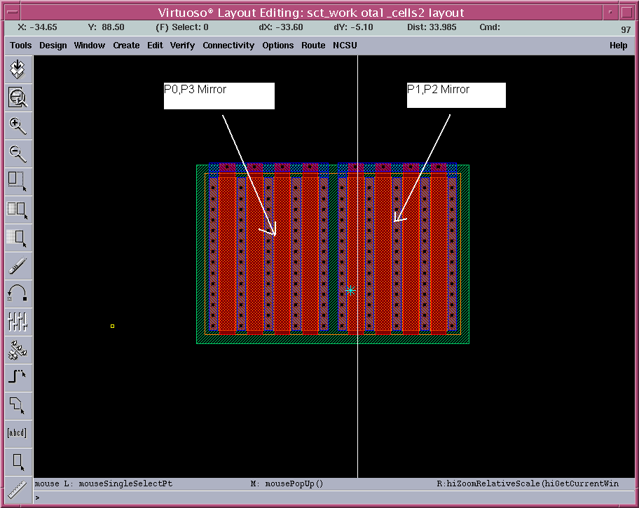
Figure 11. Layout of P0, P1, P2, P3.
Figure 12. Layout of P0, P1, P2, P3 with Annotation. C7. Substrate Plugging Now that all of the individual cells are complete, it is time to add substrate plugs. It is good to add a complete ring around each cell. It is not absolutely necessary to add the ring all the way around the differential pair, but it should help matching.
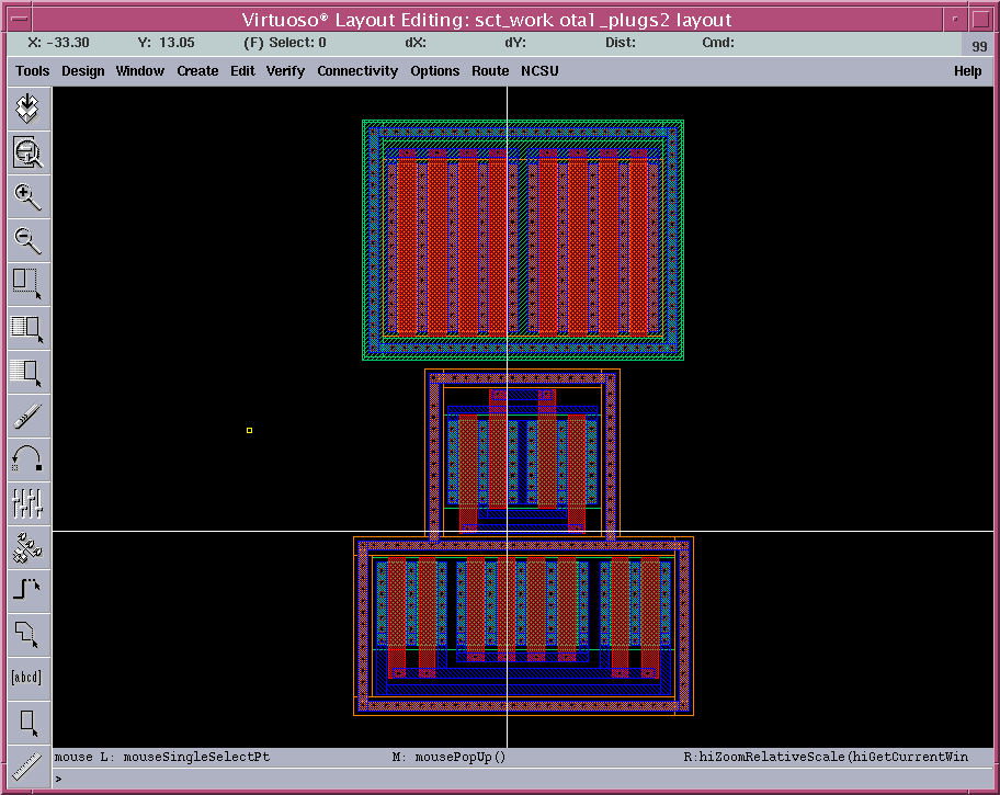
Figure 13. Layout of cells showing substrate plugs. C8. Final Routing All that is left is final routing. I routed all sources to the well ties using metal 2. All routing between cells is done with metal 2, so that the well tie can be crossed.
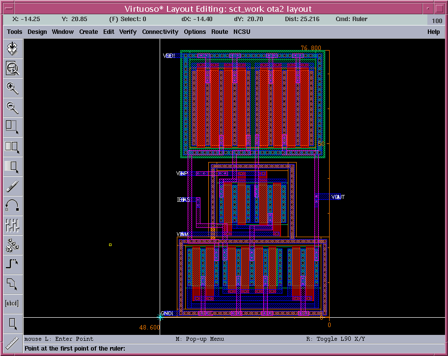
Figure 14. Complete OTA layout. D. Extraction and LVS Next extract the layout and run LVS to make sure that everything is correct. Here is my extracted view:
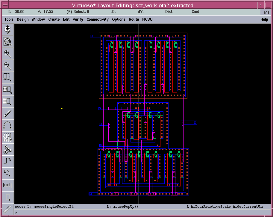
Figure 15. OTA Extraction My LVS results are here. E. Post Layout Simulation The final step is post layout simulation. My simulation file is here. Here are my simulation results.
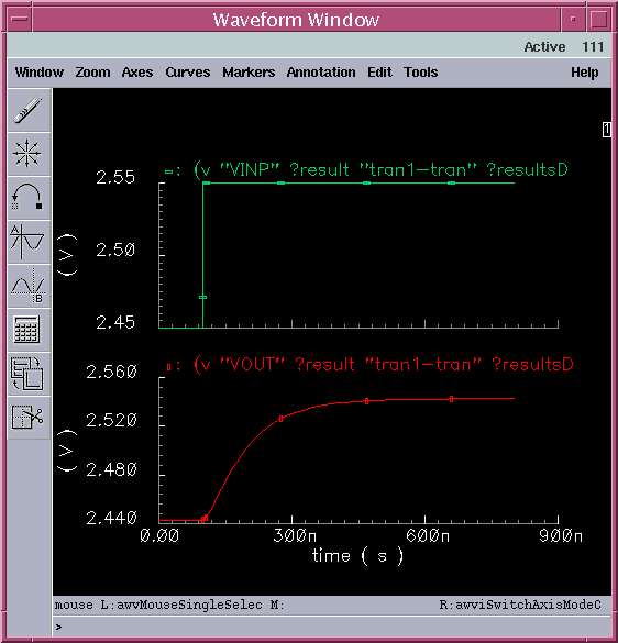
Figure 16. Post Layout Simulation A PDF version is available here.