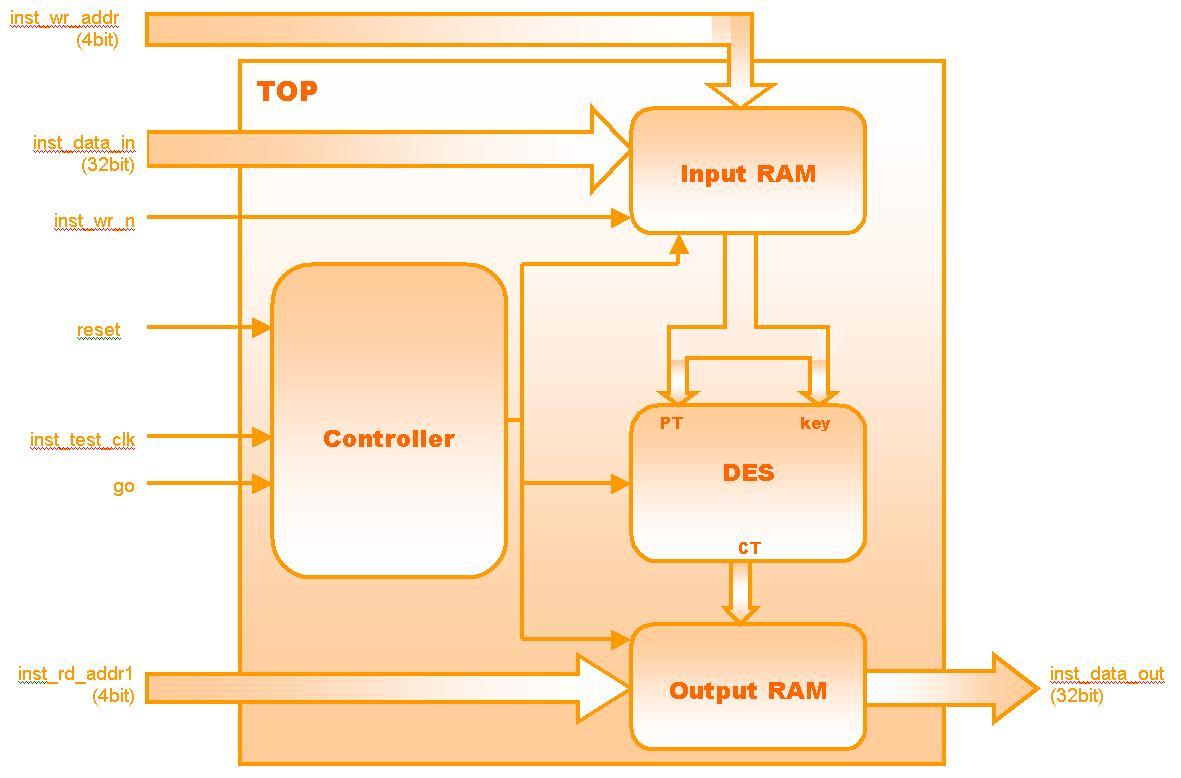
Entire
|
Figure : Entire Block Diagram |
|
| Click on the picture for a bigger picture | |
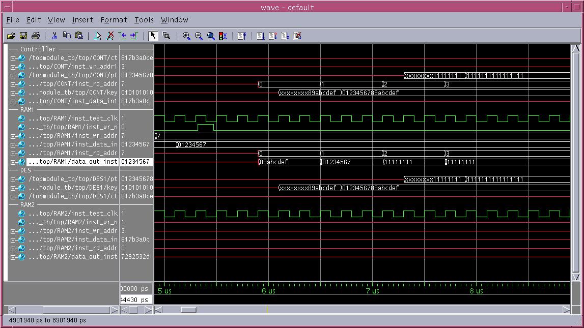
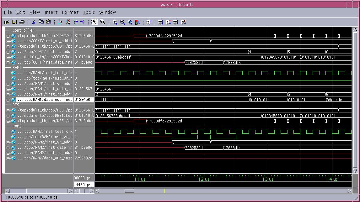
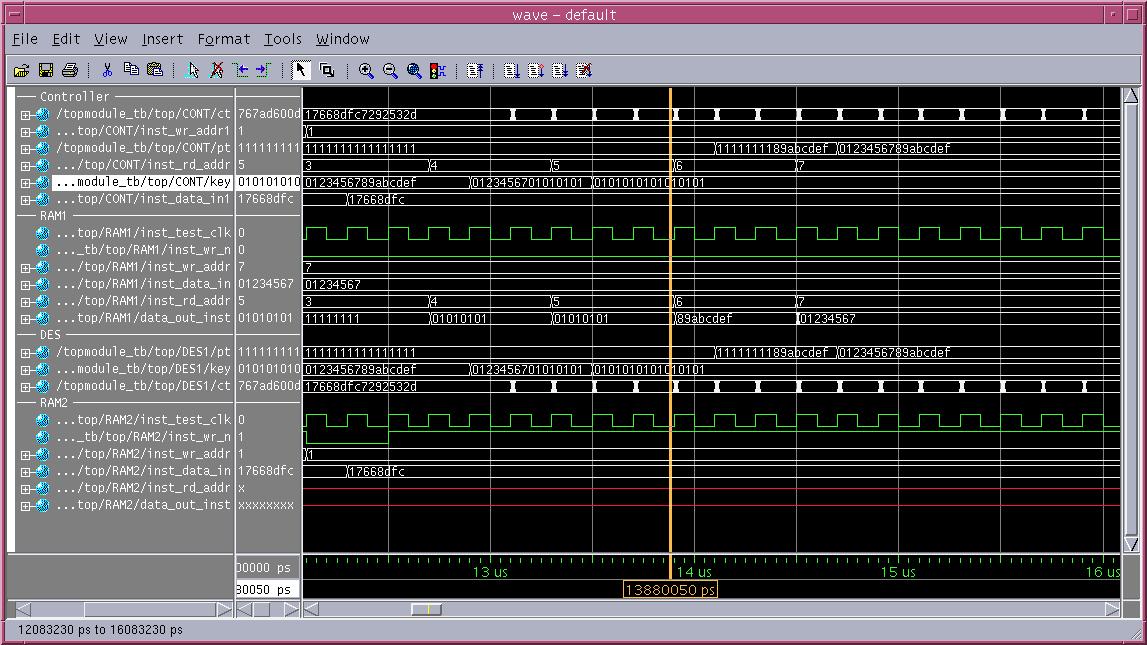
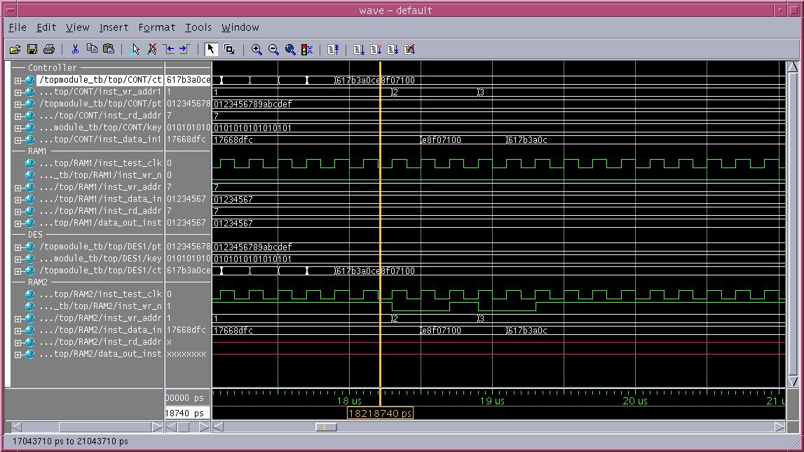
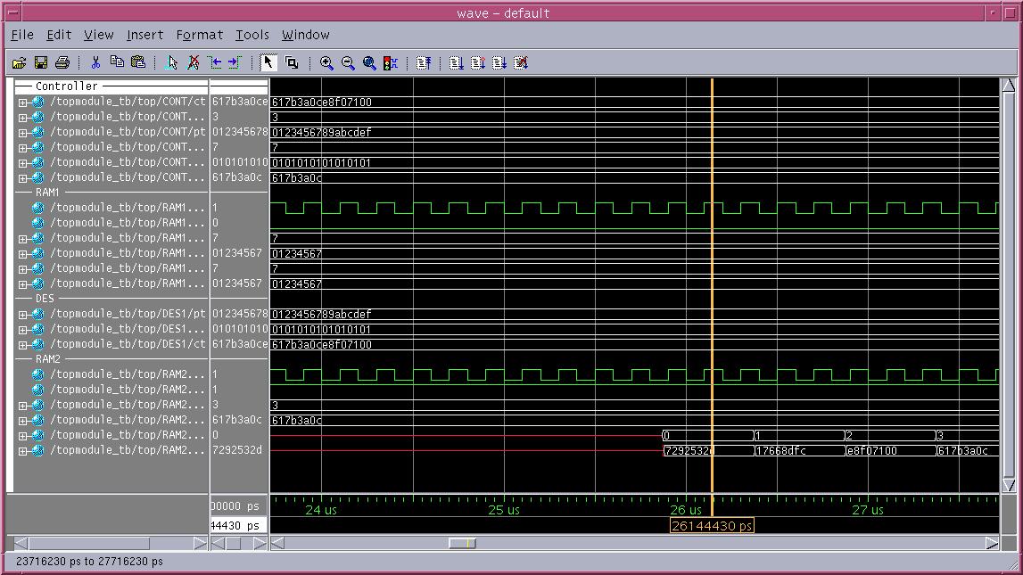
This block was simulated and these are the screenshots.
| Screenshot1 This shows the first set of key and plain text (pt) LSB and MSB being read from the input RAM. |
| Screenshot2 This shows the calculated ciphertext (ct) for the first set of data being written to the output RAM. |
| Screenshot3 This shows the second set of key and plain text (pt) LSB and MSB being read from the input RAM. |
| Screenshot4 This shows the calculated ciphertext (ct) for the second set of data being written to the output RAM. |
| Screenshot5 This shows the stored ciphertext being read from the output RAM . |
| First set of data: Key: 0123456789abcdef (hex) Plaintext: 1111111111111111 (hex) |
| Expected ciphered text output:17668dfc7292532d(hex) |
| Second set of data: Key: 0101010101010101 (hex) Plaintext: 0123456789abcdef (hex) |
|
Expected ciphered text output: 617b3a0ce8f07100 (hex) |
|
The pre layout simulation results match the expected results. |