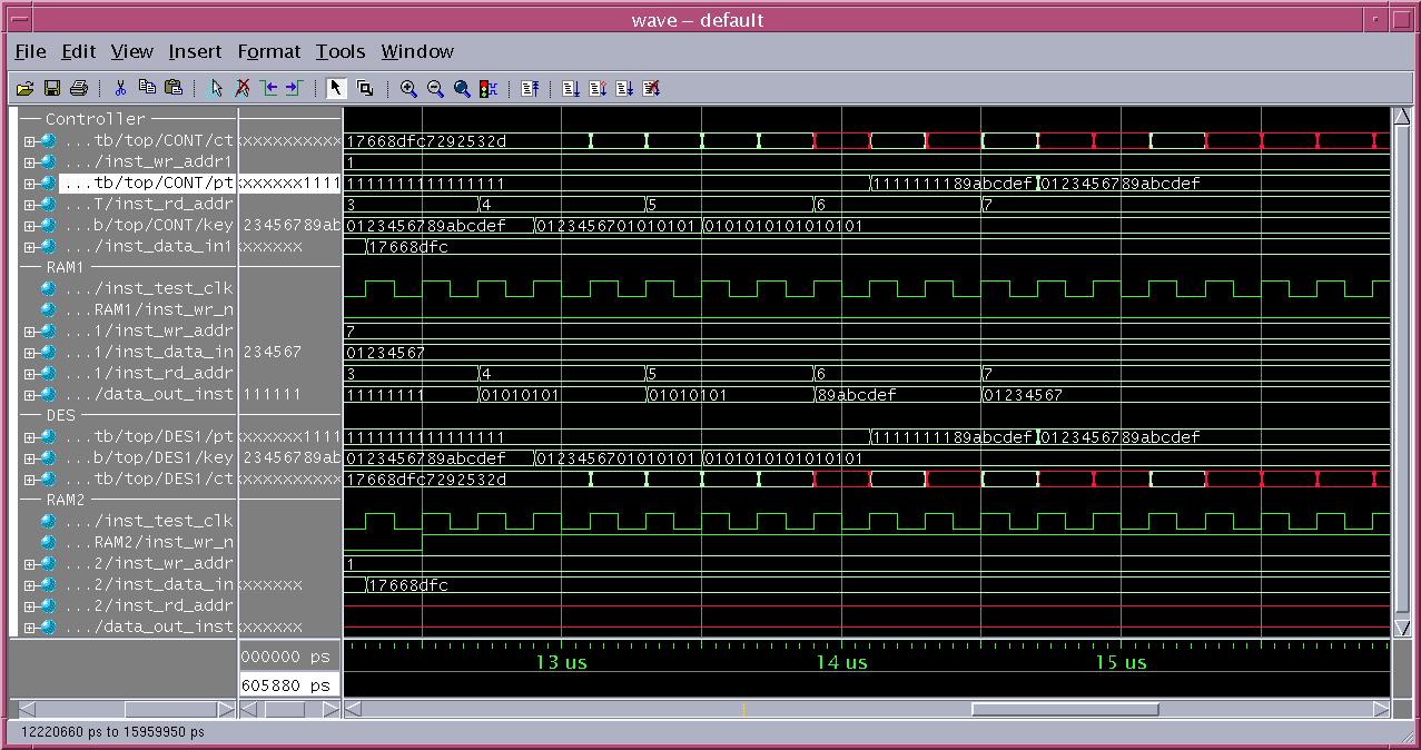
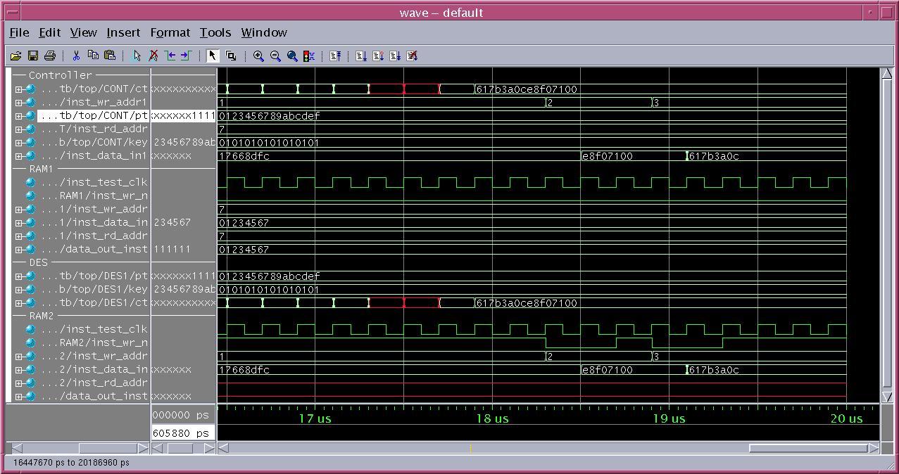
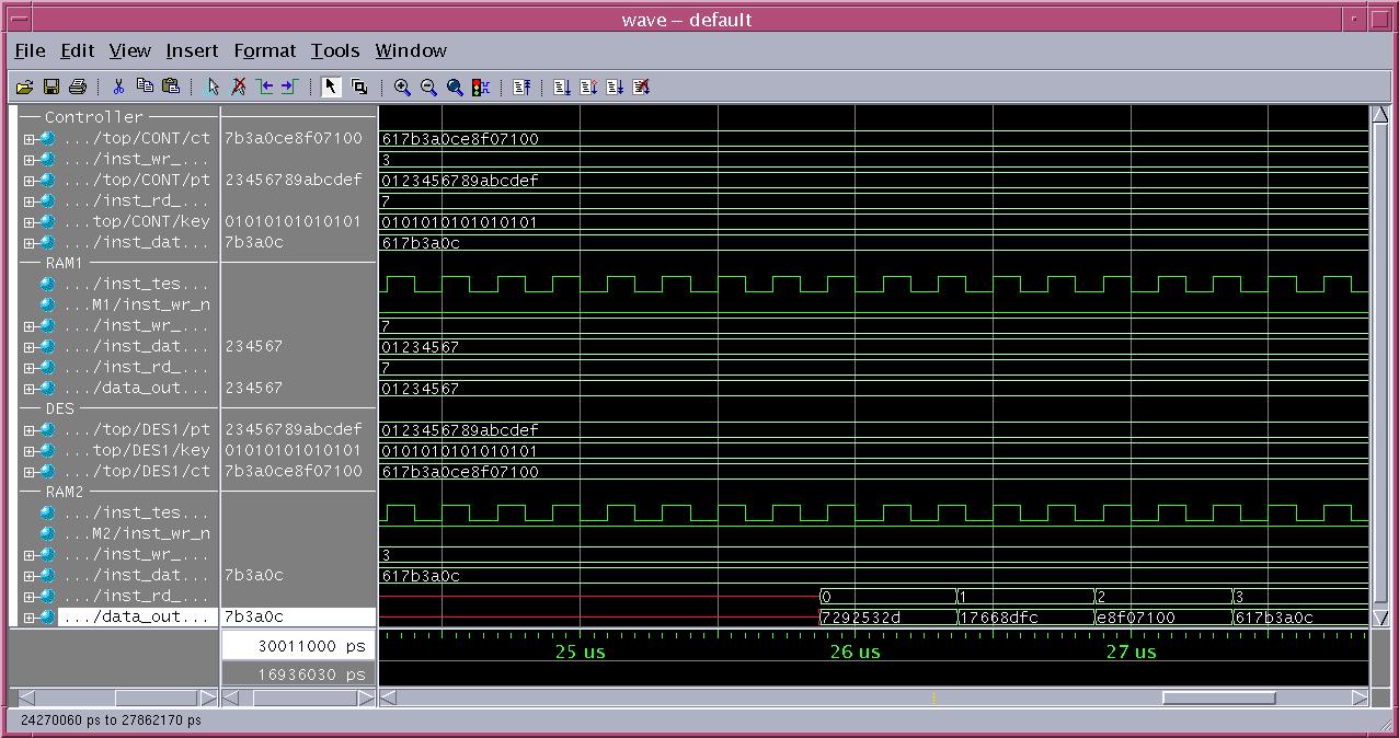
| The following Screen Shots show the Post-Layout simulation of the entire block with the SDF file included which takes into account the delays while simulation. |
| This shows a set of data being read from the input RAM and transfer to the DES Block - ScreenShot |
| This shows the cipher text from the above set of data - ScreenShot |
| This shows the cipher text being written into the output RAM - ScreenShot |
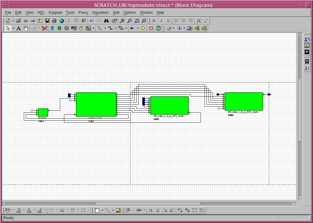
| The following is the entire module containing Input RAM -> DES --> Output RAM |
| Block Diagram |
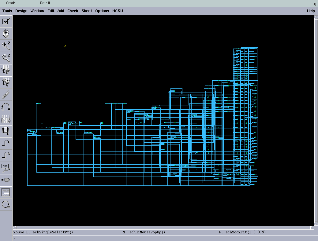
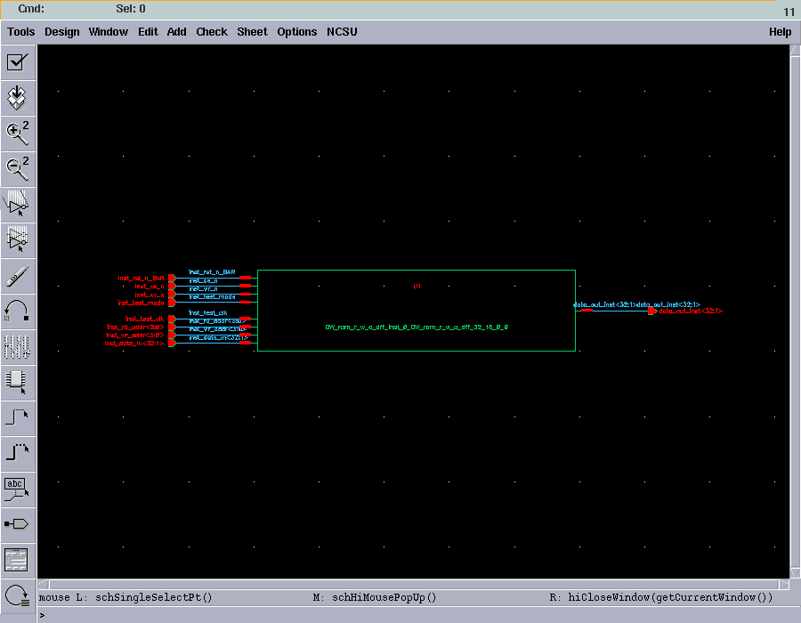
| The following figure is the view of the entire block diagram. |
|
|
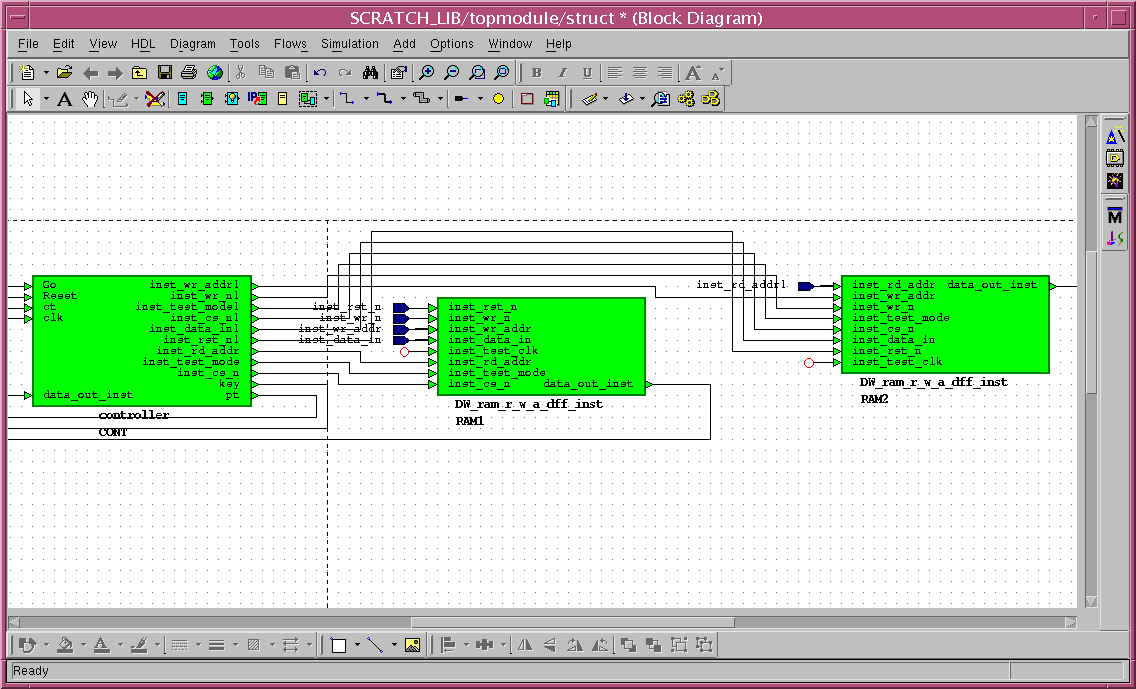
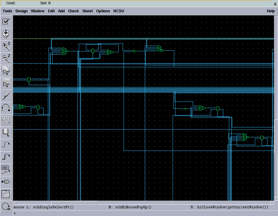
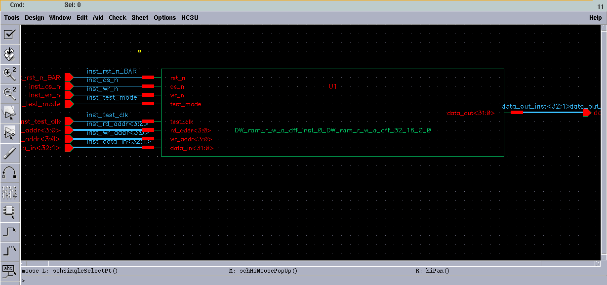
| The following is the zoomed view |
|
|
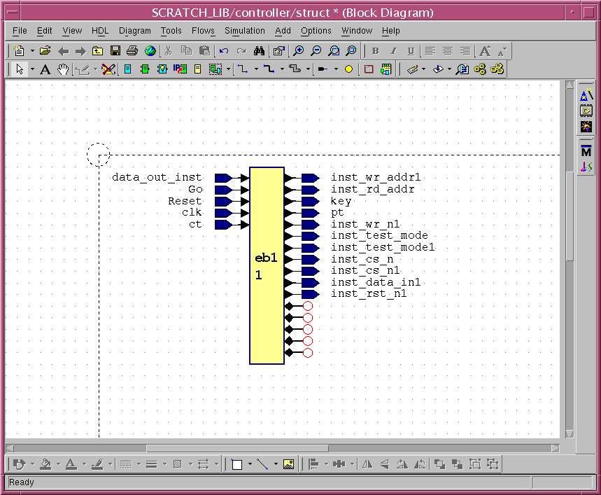
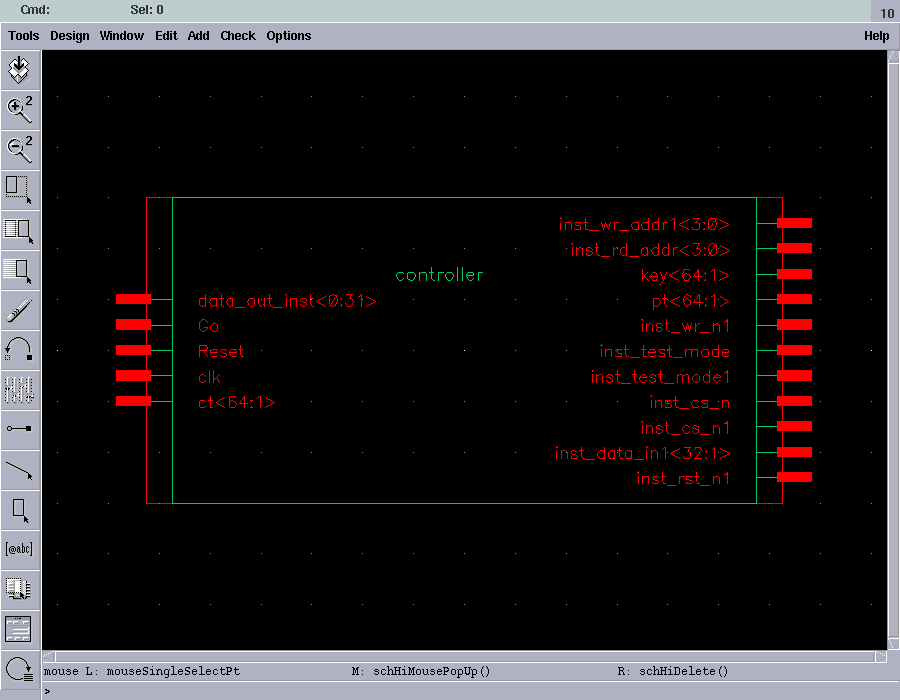
| Controller |
| Controller module houses the State machine that is responsible for reading the values from RAM and giving the GO signal to start the DES module and also writes the values from DES to the Second RAM The following figure is the view of the controller module |
|
|
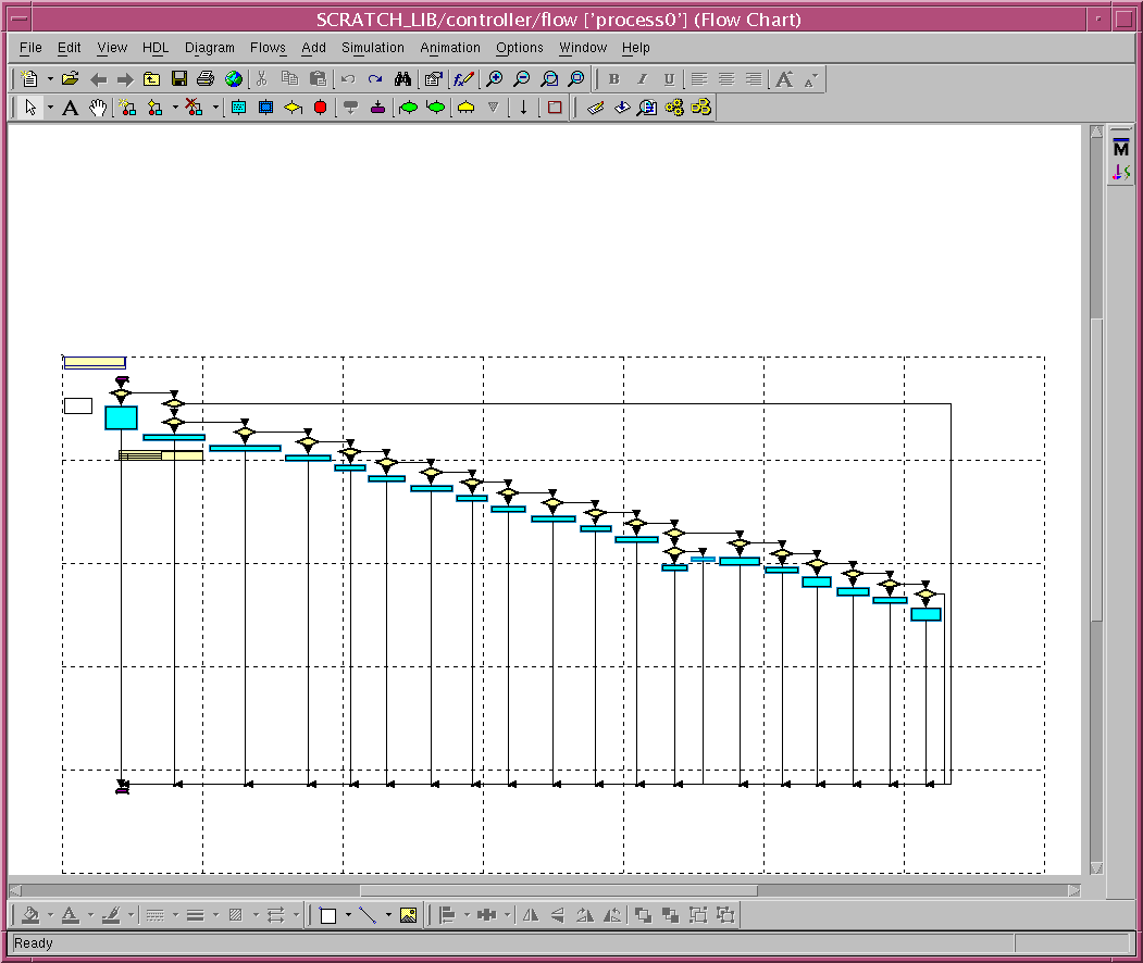
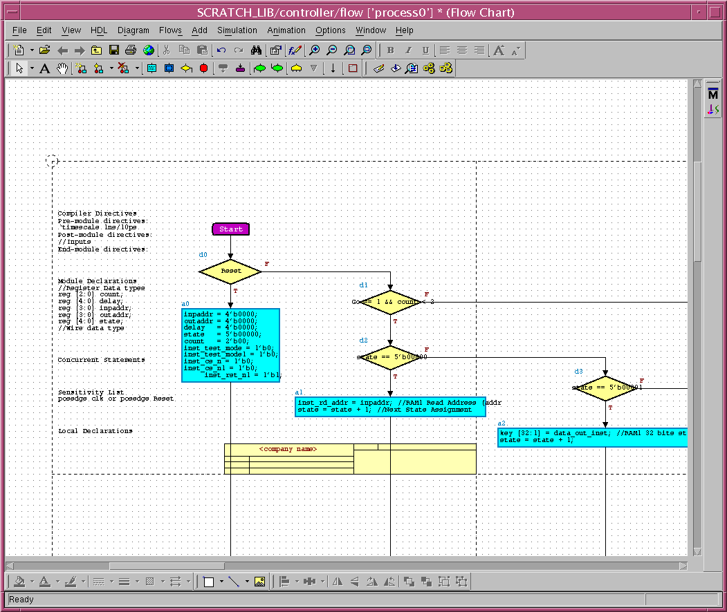
| The following is the State machine flow in the controller module |
|
|
| The following is the State machine flow(zoom) in the controller module |
|
|
| RAM |
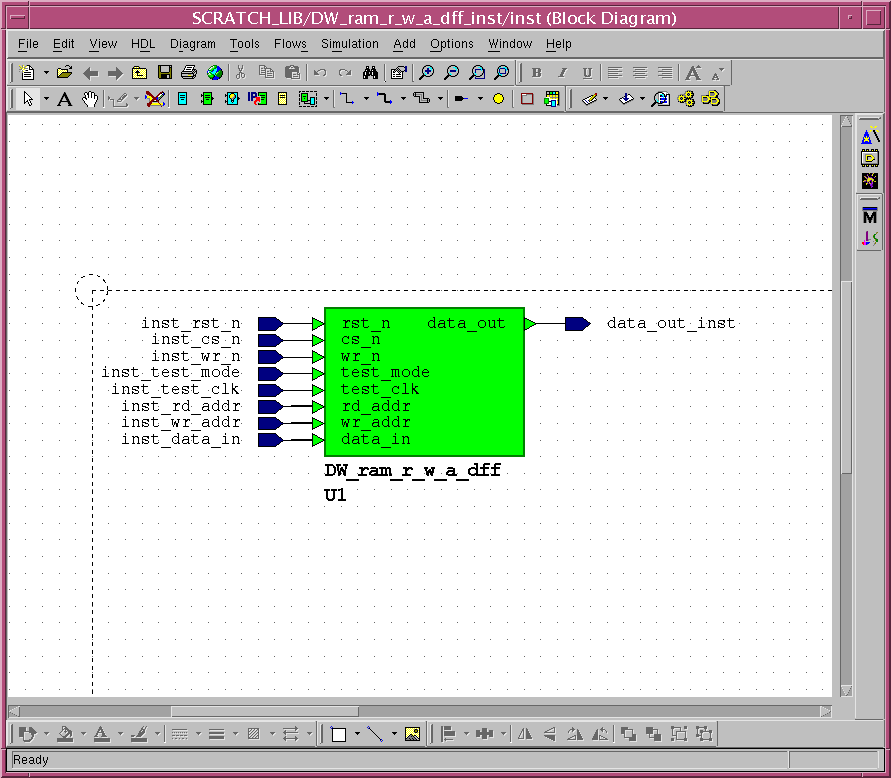
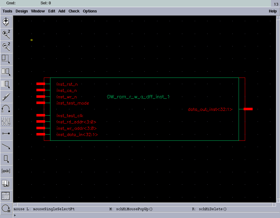
| The following figure shows the Input RAM |
|
|
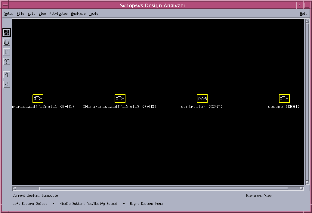
| Synthesis results of the Entire module |
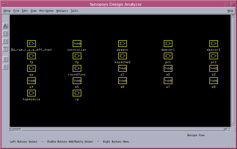
| The following figure shows the different modules in the project as an outcome of Design Analyzer |
|
|
| Schematic ,Symbolic and Hierarchical views of Individual modules |
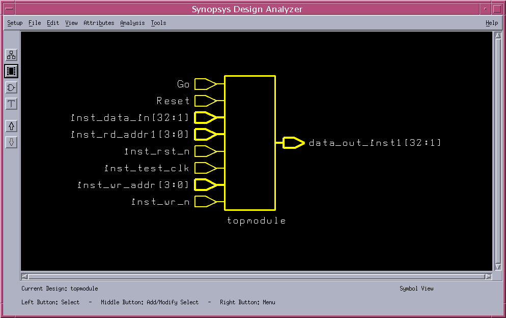
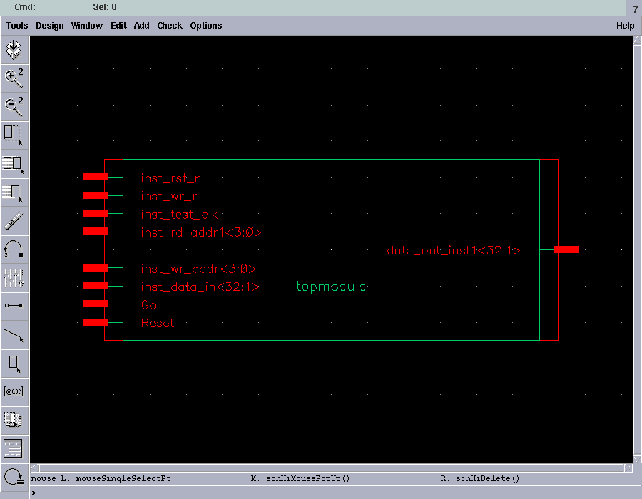
| Top Module |
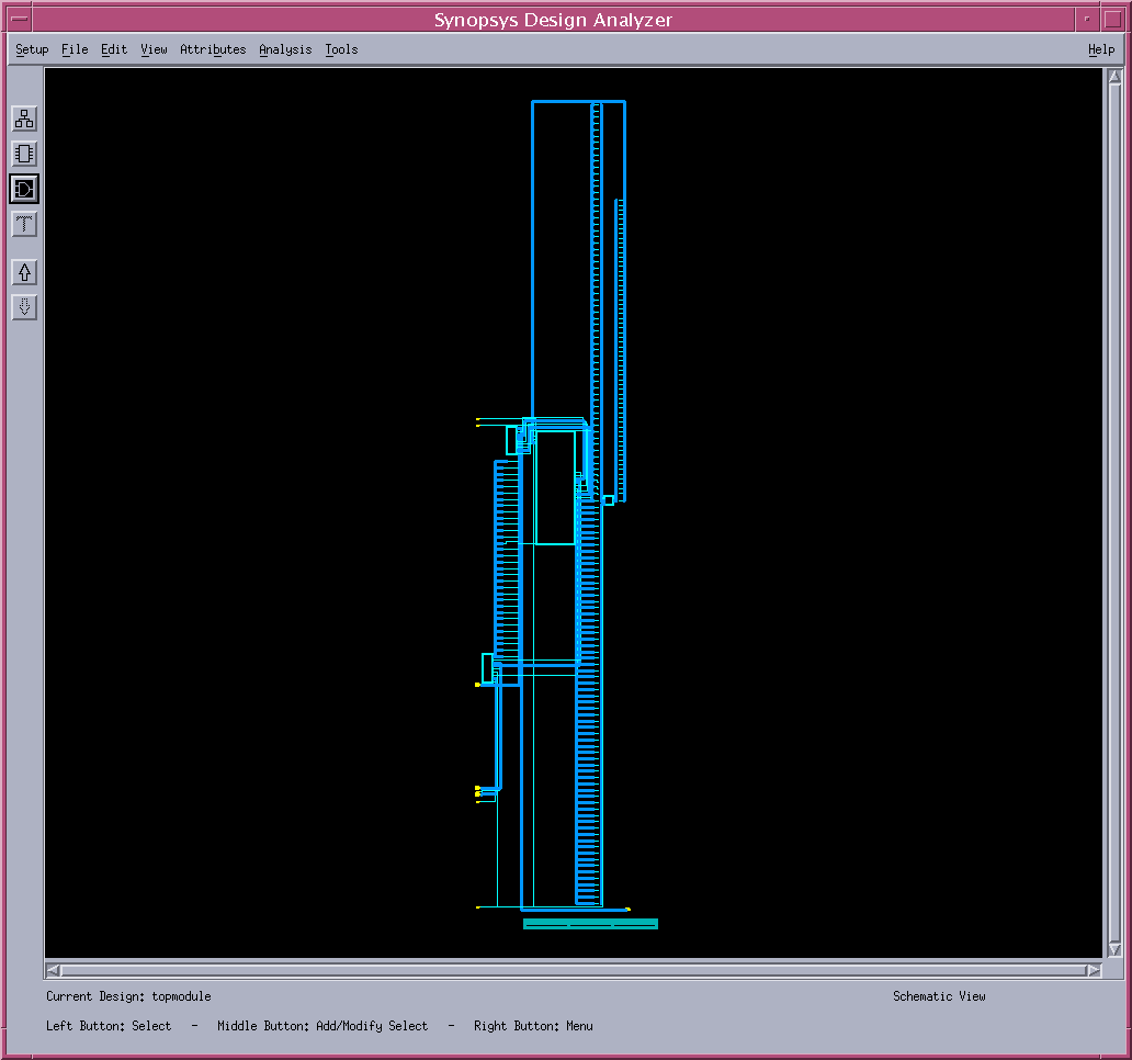
| The following figure shows the Schematic view of the Entire top module |
|
|
| The following figure represents the Symbolic view of the Entire top module |
|
|
| The following figure shows the Hierarchical view of the Entire top module |
|
|
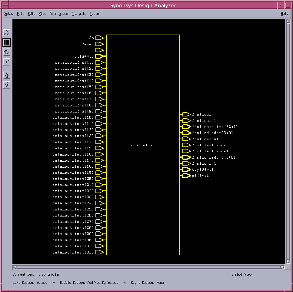
| Controller |
| The following figure represents the Symbolic view of the Controller module |
|
|
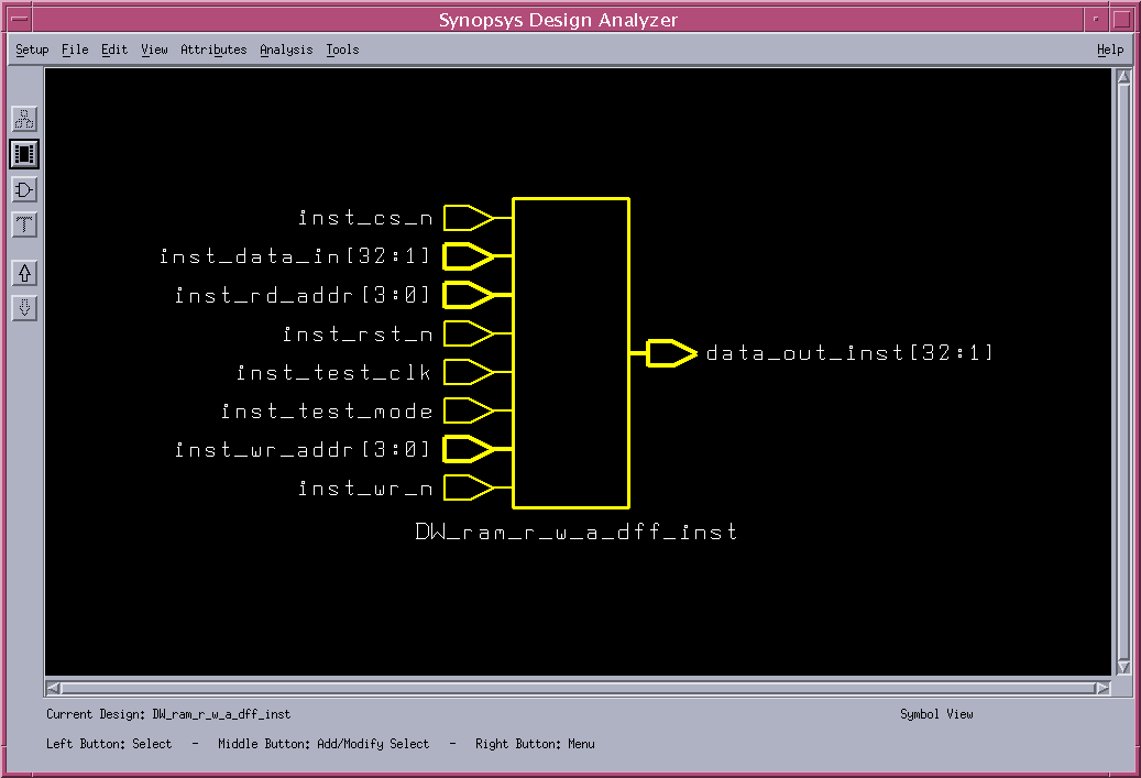
| RAM |
| The following figure shows the Schematic view of the RAM module |
|
|
| The following figure represents the Symbolic view of the RAM module |
|
|
| Layout |
| Once the gate-level netlist is obtained using design compiler it is then
given as one of the inputs to silicon ensemble to do the automatic place and routing. A global constraint file (gcf) is also imported in silicon ensemble to get Standard delay format (SDF) of the cells and the interconnects |
| Silicon Ensemble |
| The following is the output from silicon ensemble. This shows the abstract view of the entire project modules |
|
|
|
The following is the floorplan report obtained by Silicon ensemble |
| Layout using ICFB |
| Once the abstract view is obtained from silicon ensemble in the form of DEF, it is then imported into ICFB to get the layout. |
| The following figure represents layout |
|
|
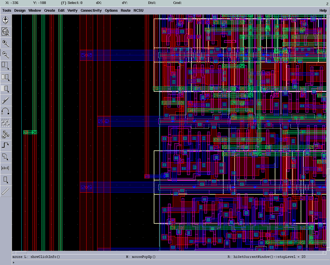
| The following shows the zoomed view |
|
|
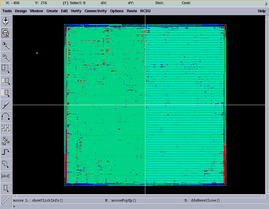
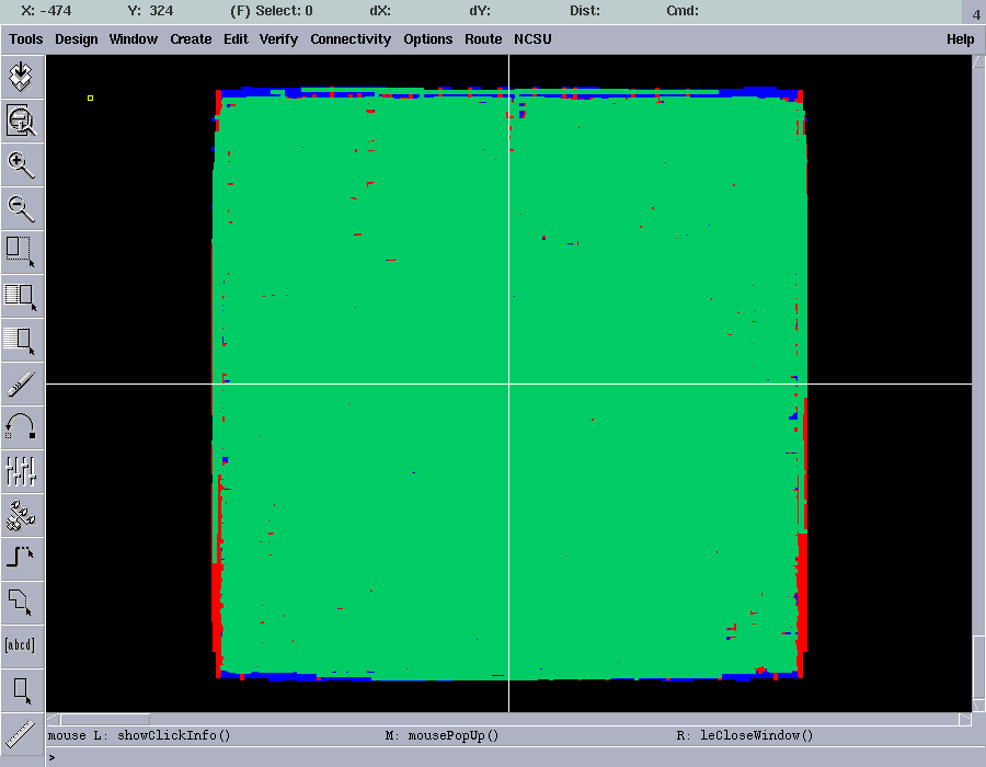
| The following figure represents the extracted view |
|
|
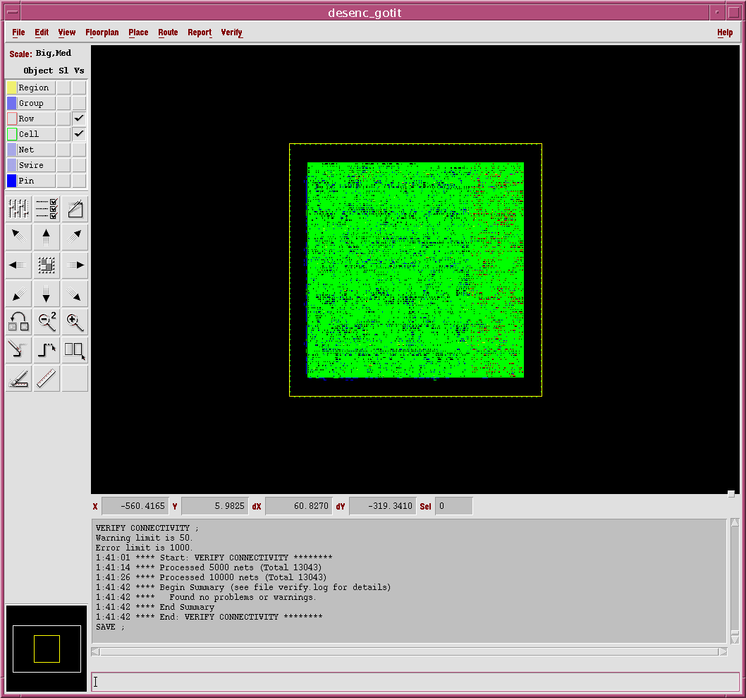
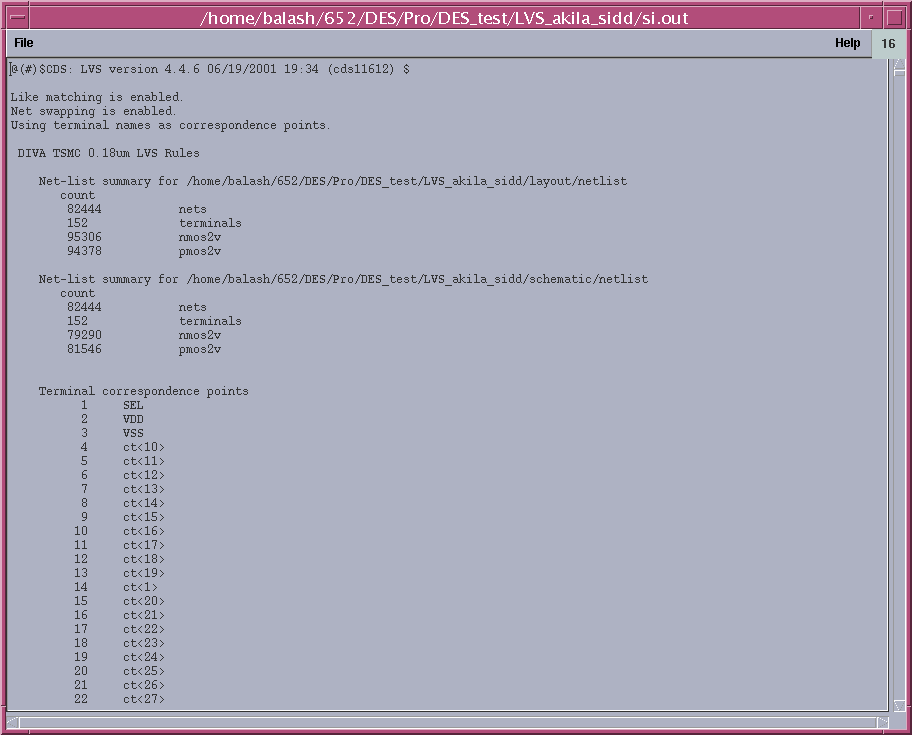
| LVS check is performed on the Extraction and Schematic (obtained from gate-level netlist). The following figure represents the LVS output. |
|
|
| Schematic obtained from Gate-Level Netlist |
| Top module |
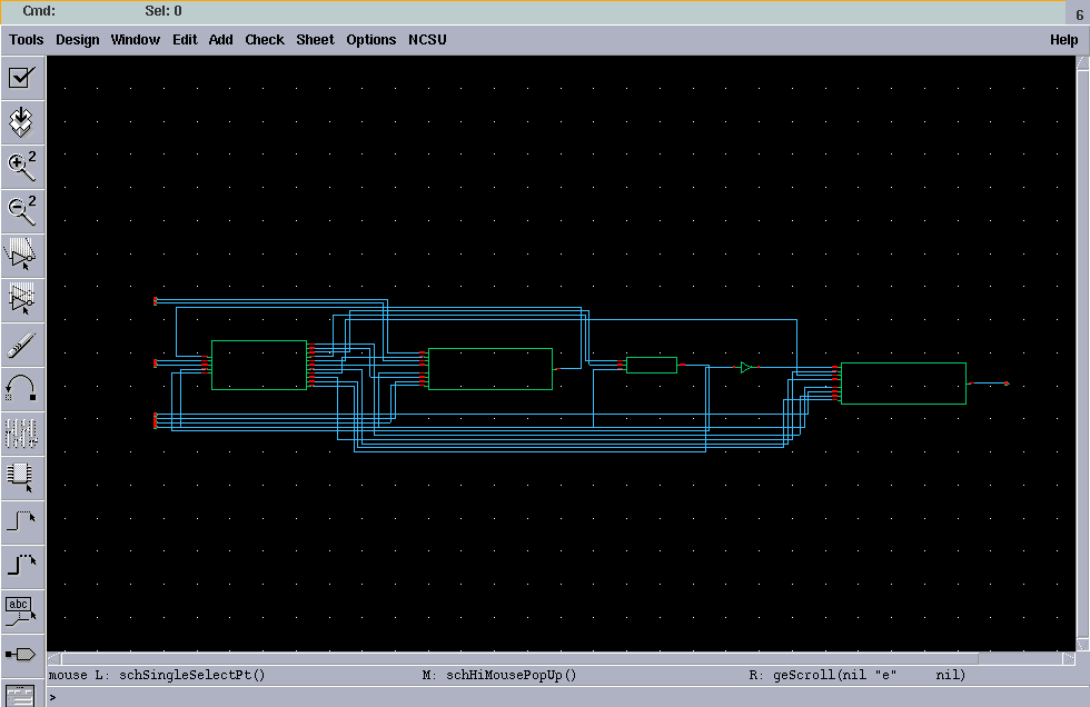
| The following figure represents Schematic view of Top module |
|
|
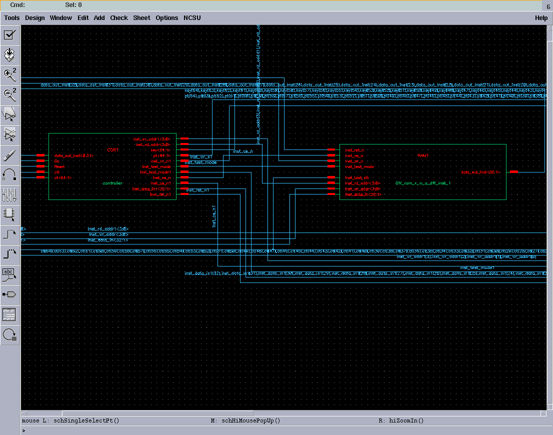
| The following figure represents zoomed view of the Schematic |
|
|
| The following figure represents symbolic view of the Top module |
|
|
| Controller |
| The following figure represents Schematic view of Controller module |
|
|
| The following figure represents zoomed view of the Schematic |
|
|
| The following figure represents symbolic view of the Controller module |
|
|
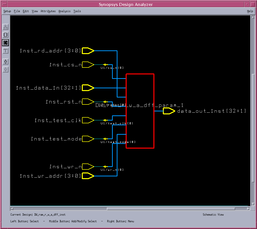
| RAM |
| The following figure represents Schematic view of RAM module |
|
|
| The following figure represents zoomed view of the Schematic |
|
|
| The following figure represents symbolic view of the RAM module |
|
|