DES
| Targeting DES to FPGA |
| The DES module is targeted to Xilinx's
virtex 1000e.
|
| Result of FPGA compiler |
| Synopsys's FPGA compiler is used to synthesize the DES module in order to target to the Xilinx' Chip. |
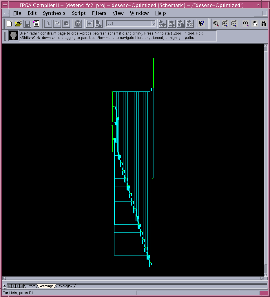
| The following figure shows the View of DES obtained using FPGA compiler. |
|
|
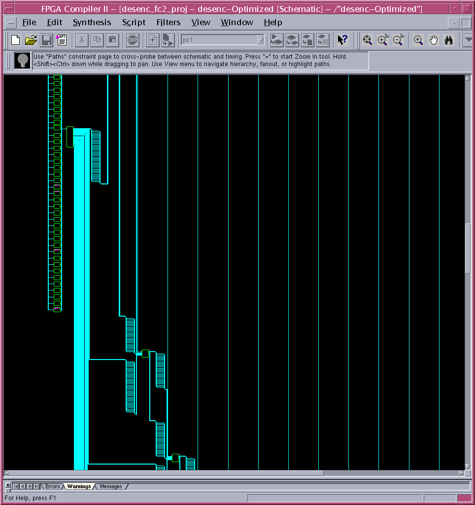
| The following figure shows the zoomed view. |
|
|
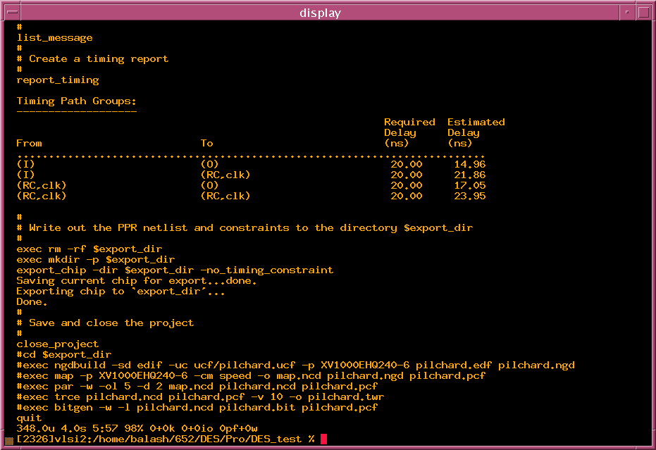
| The following is the result obtained using the FPGA compiler |
|
|
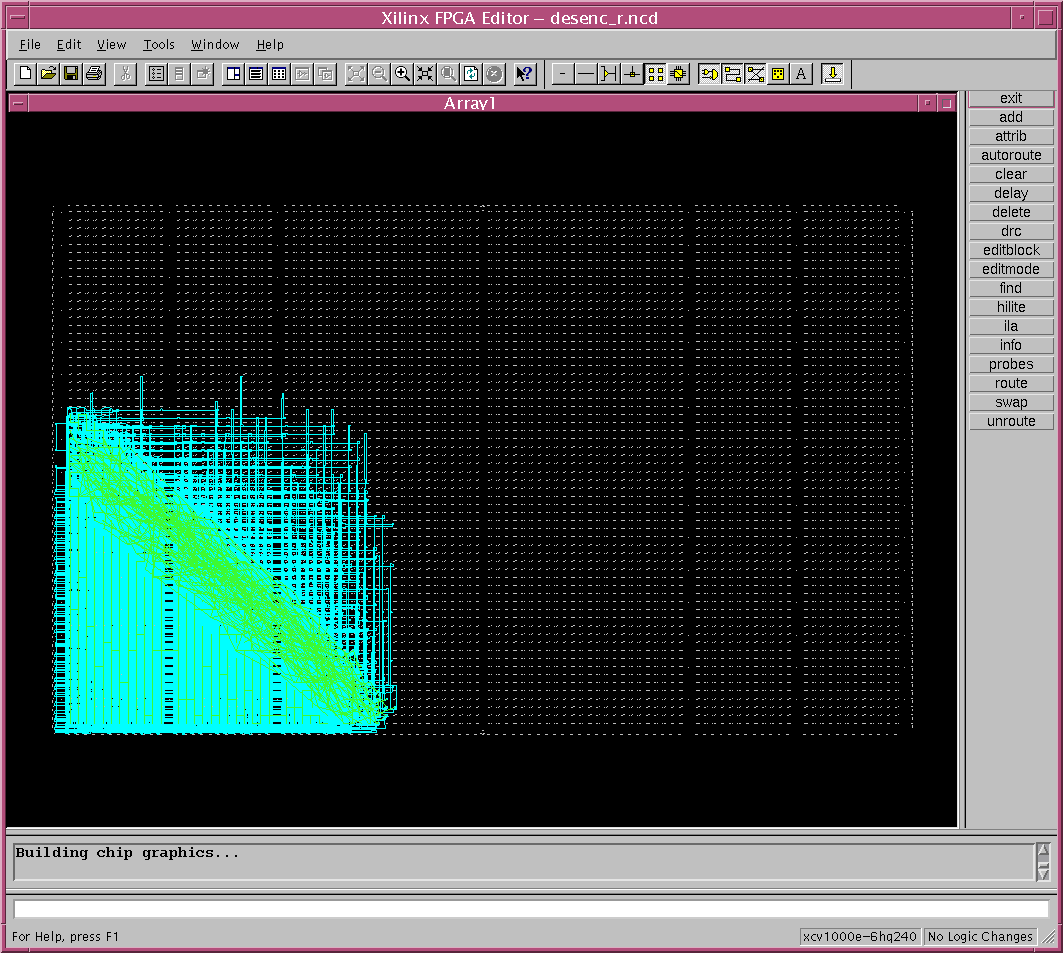
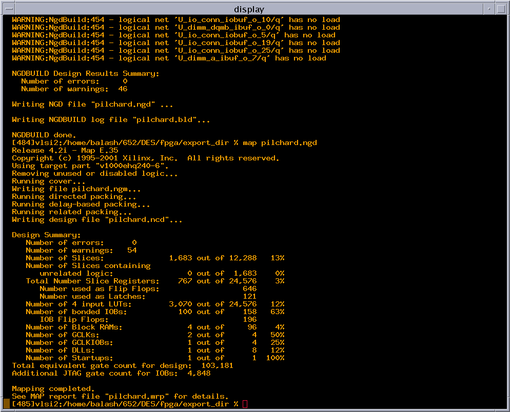
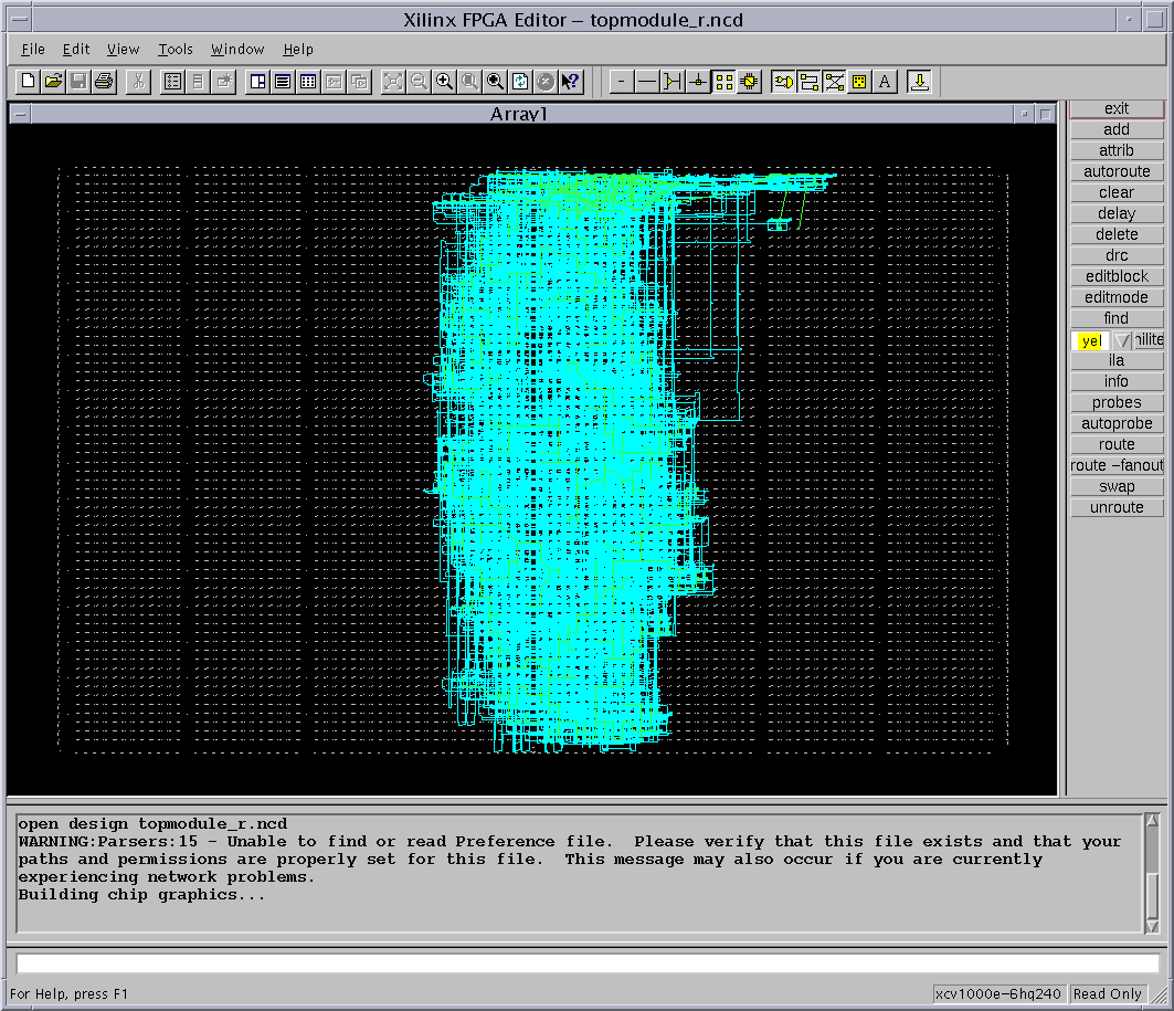
| Place and Route |
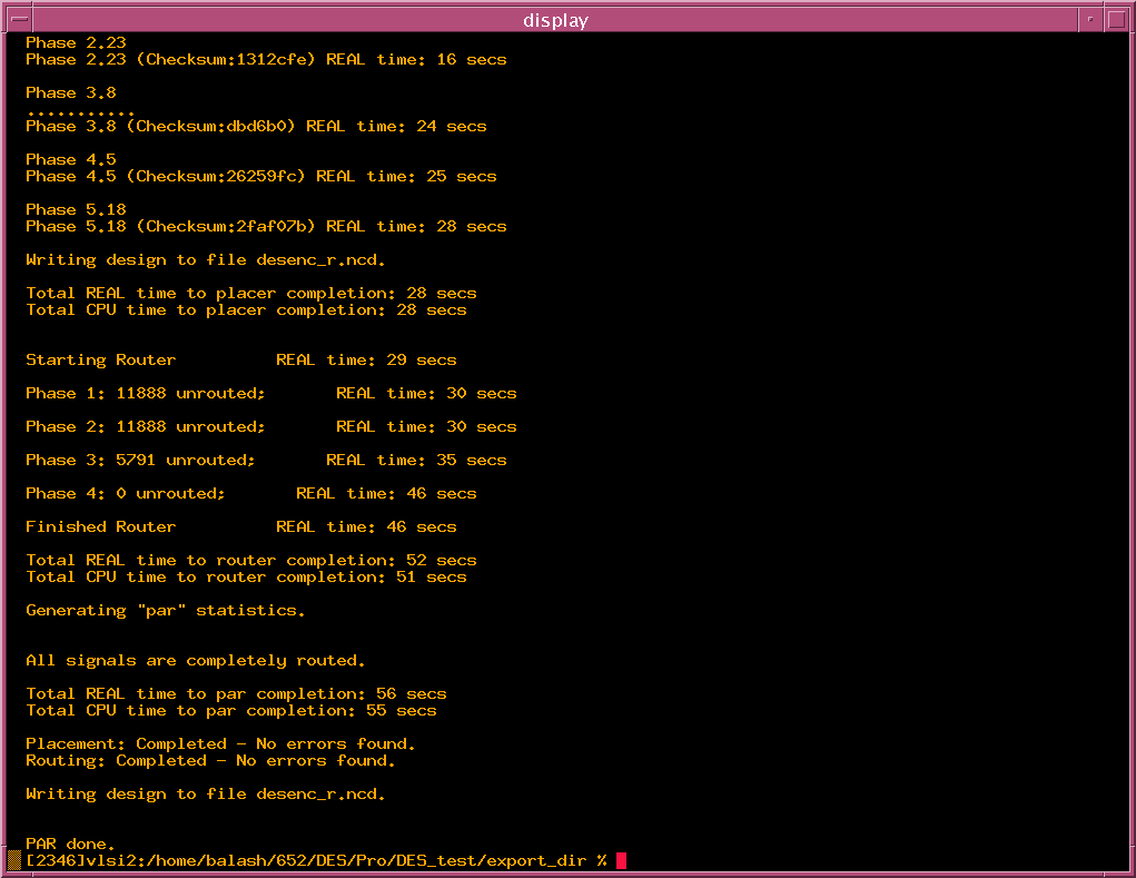
| Xilinx Place and Route program was used to map the DES design in the chip followed by Placing and Routing . |
| The following figure shows the Place and Route results. |
|
|
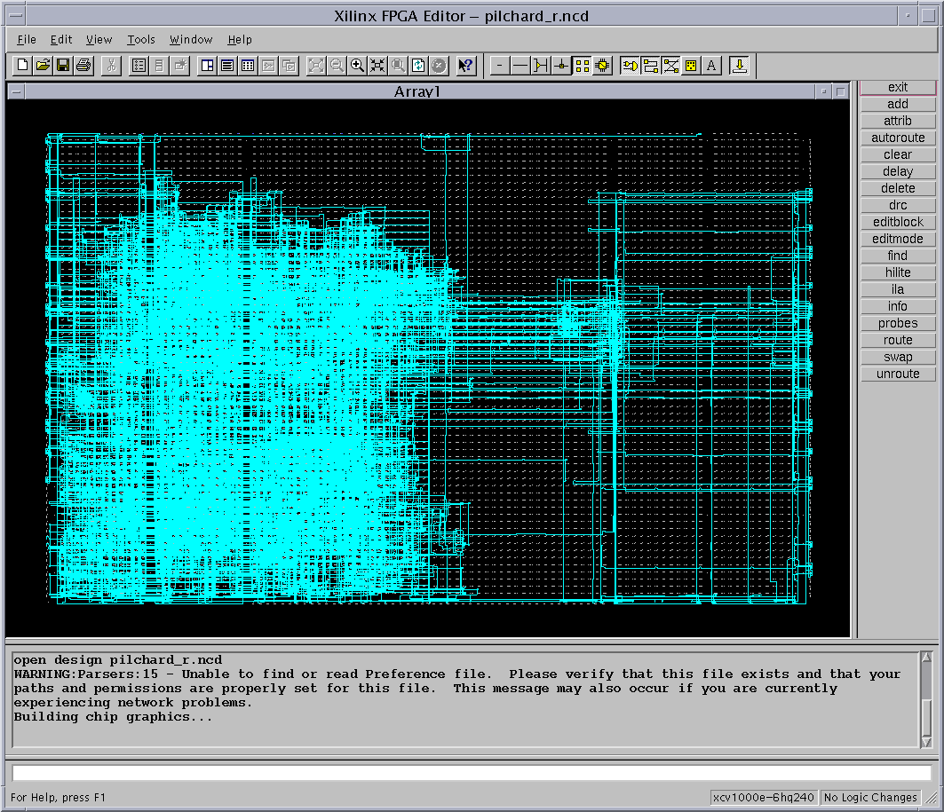
| The following figure shows the Layout. |
|
|
| DES interfaced with Xilinx's coregen |
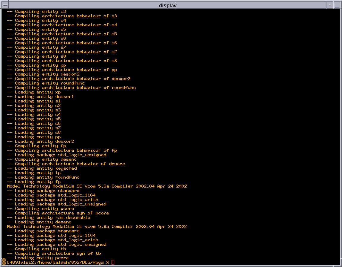
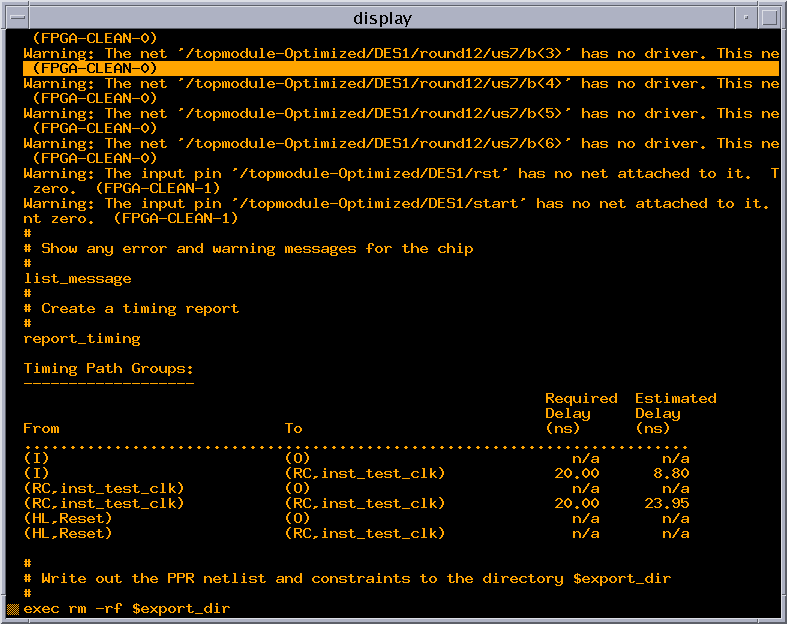
| The idea here is to have one dual-port RAM and the DES module gets its values from it. Once the DES module calculates the ciphered text , it would be put back into to same RAM. The following figure shows the compile log of pre-layout simulation |
|
|
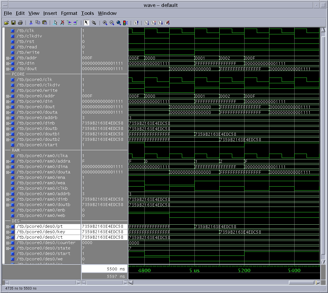
| The following figures shows the Pre-layout simulation |
|
|
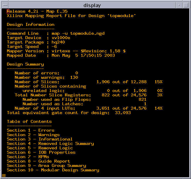
| Synthesis Results |
| FPGA compiler was used to synthesize the entire block. The following is the synthesis result |
|
|
| The following is the mapping result |
|
|
| The following shows the layout of the entire block (DES+xilinx coregen) on the Virtex 1000E |
|
|
| DES interfaced with Synopsys' Designware RAM |
| Mapping of the Entire DES with the Designware RAM was done on Xilinx's virtex 1000E. |
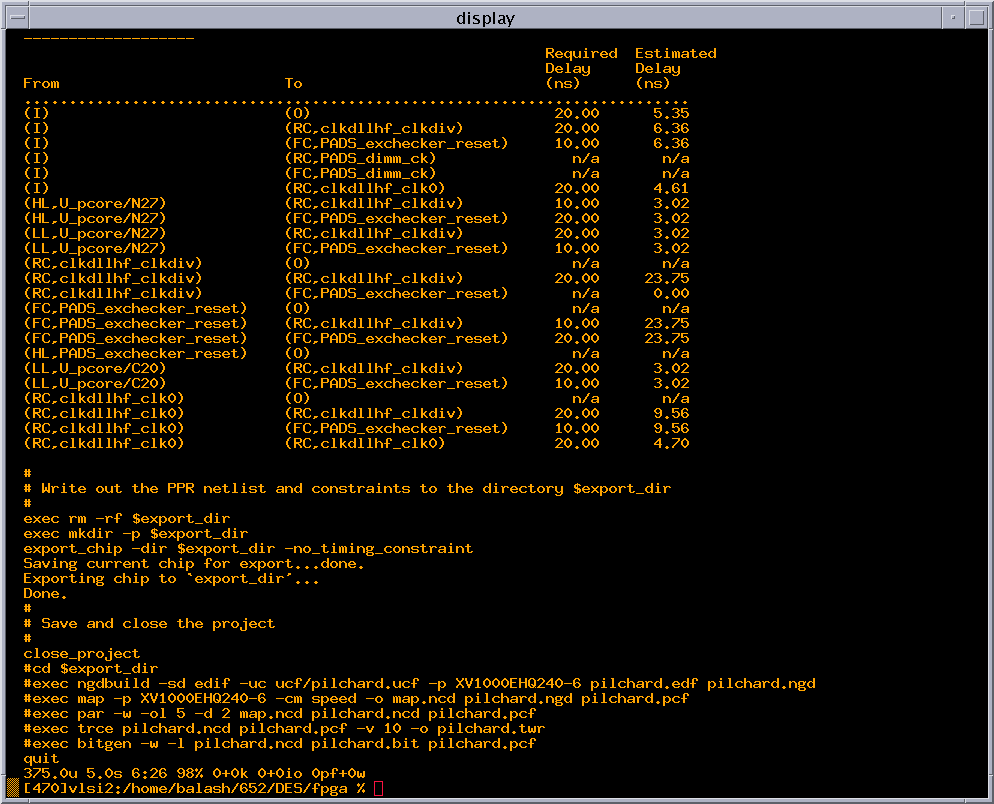
| The following is the Synthesis results |
|
|
| The following is the mapping results |
|
|
| The following is the layout |
|
|