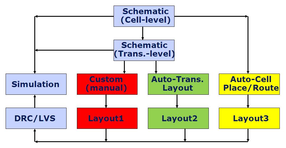
Macro and Leafcell Properties
A macro consists of two or more leafcells.
A soft-macro can be "hypenated" or decomposed for global optimization
whereas a hard-macro or leafcell is fixed to preserve area/delay.
This semester we will compare 3 methods for implementing layouts:
(Silicon Ensemble has been replaced by SoC Encounter.)
Encounter Reference Manual (10 MByte pdf)
Place & Route for FreePDK45nm
Layout with cells placed and then with 4 metal layers routed:
General Procedure
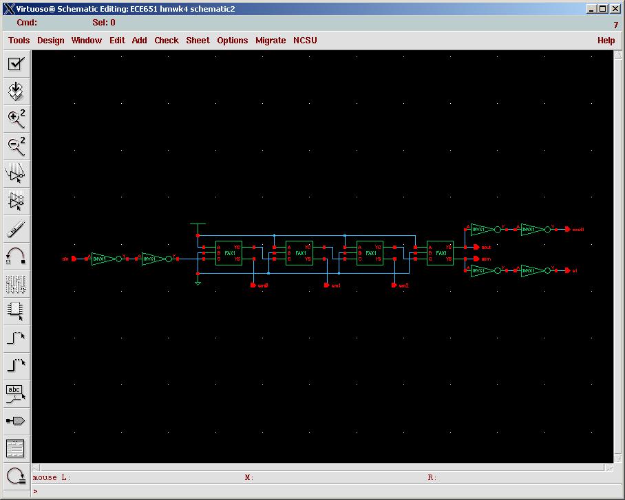
1. Invoke icfb and use Composer to draw a schematic which uses multiple leaf_cells.
2. Generate the net-list for Spectre.
3. Simulate pre-layout using Spectre.
4. Use SOC_Encounter to perform placement and routing automatically and to produce the DEF file.
2009 students: Skip steps 5-8.
5. Use Virtuoso to read in the DEF file, add pins for gnd! and vdd!
(Notes: Skip to page 4 and in the command window, perform "Import-def".
(On page 7, replace "Replace-All" with "Apply, then Replace-All".)
6. Perform DRC.
7. Extract the cell and compare LVS.
8. Simulate post-layout using Spectre.
Execute the following:
1. login to ada3.eecs.utk.edu
2. mkdir 651-hw6
3. cp ~bouldin/webhome/protected/651-hw6.tar 651-hw6
4. cd 651-hw6
5. tar -xvf 651-hw6.tar
6. cd 651-hw6
7. ls
You should have the following files:
osu05_stdcells.stacks.lef*
osu05_stdcells.tlf*
osu05_stdcells.v*
parta.v
parta_script*
partb.v
partb_script*
partc.v
partc_script*
Note: The full structural verilog info with delays for each OSU standard cell
can be found on ada3 at:
/usr/local/osu/lib/ami05/OSU_stdcells_ami05/*/functional/verilog.v
where * = AND2X1, FAX1 etc.
Part A (NAND):
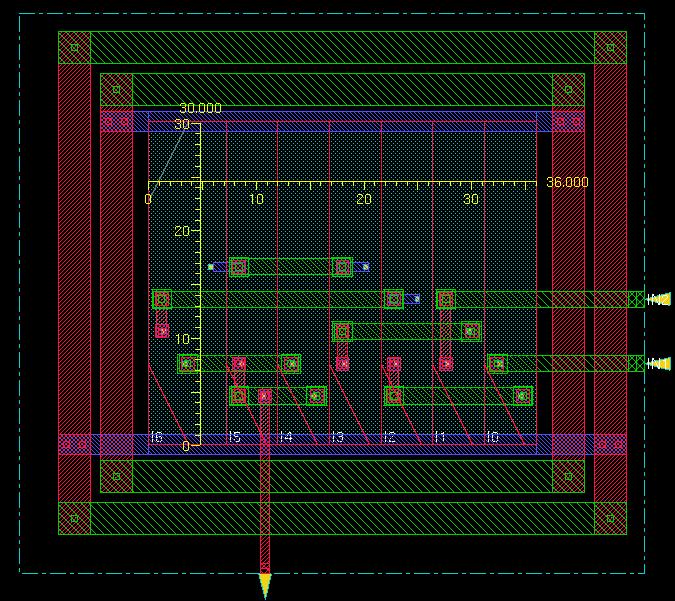
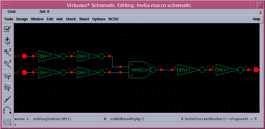 Note in parta_script: floorPlan -r 0.5 1.0 10 10 10 10
(Floorplan options: aspect ratio of H/W; core utilization)
8. encounter
NOTE: Type the following in the terminal window:
encounter 1> source parta_script
The results will be displayed in the encounter GUI window.
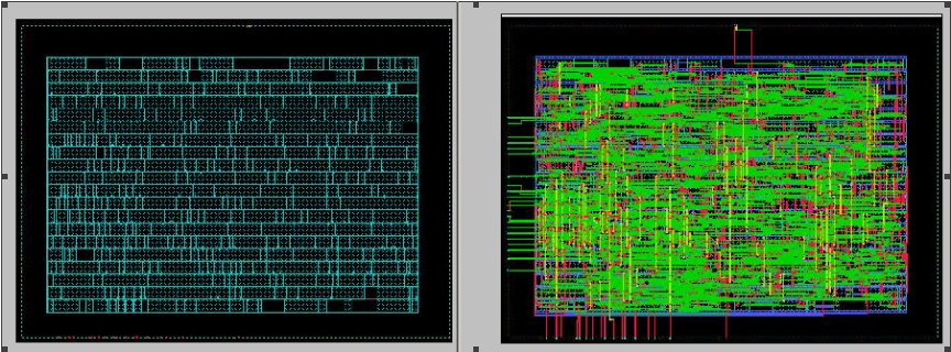
Capture the layout which in my case is 30u high and 36u wide:
2007:
Note in parta_script: floorPlan -r 0.5 1.0 10 10 10 10
(Floorplan options: aspect ratio of H/W; core utilization)
8. encounter
NOTE: Type the following in the terminal window:
encounter 1> source parta_script
The results will be displayed in the encounter GUI window.
Capture the layout which in my case is 30u high and 36u wide:
2007:
 2008 and 2009:
 encounter 2> exit
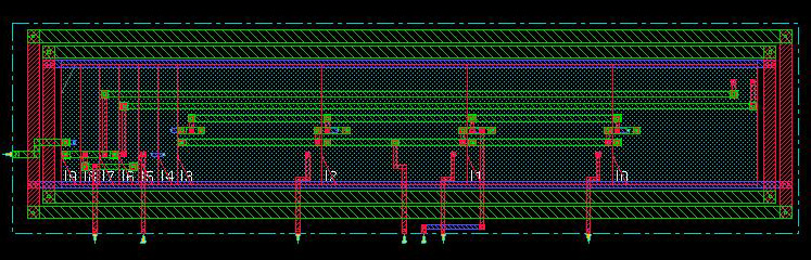
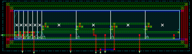
Part B (one row 4-bit ADDER like hw4-case 2):
 Note in partb_script: floorPlan -r 0.5 1.0 10 10 10 10
9. encounter
encounter 1> source partb_script
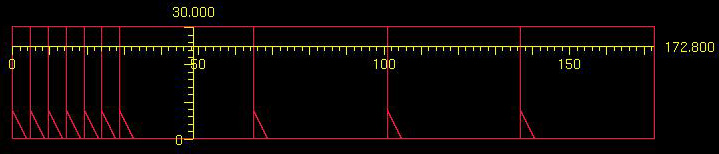
capture the layout which in my case is 30u high and 172.8u wide:
2007:
Note in partb_script: floorPlan -r 0.5 1.0 10 10 10 10
9. encounter
encounter 1> source partb_script
capture the layout which in my case is 30u high and 172.8u wide:
2007:
 2007:
2007:
 2008 and 2009:
 encounter 2> exit
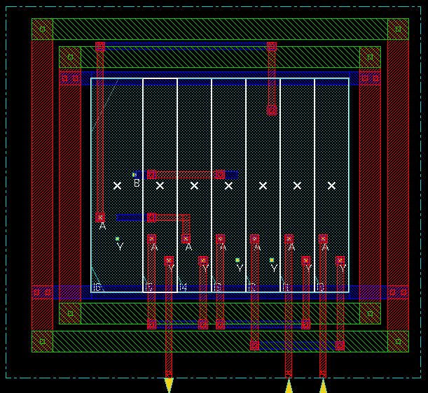
Part C (square 4-bit ADDER like hw4-case 2 using two rows):
Note in partc_script: floorPlan -r 0.8 0.95 10 10 10 10
10. encounter
encounter 1> source partc_script
capture the layout which in my case is 60u high and 88.8u wide:
2007:
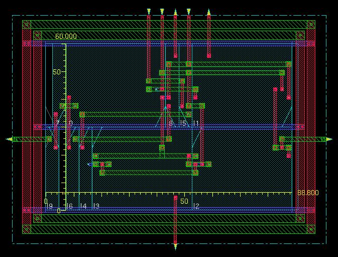 2008 and 2009:
 encounter 2> exit
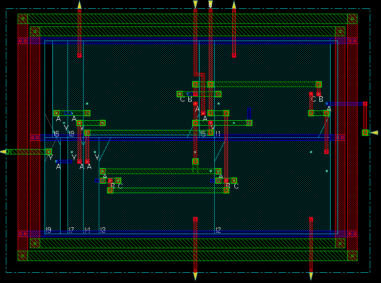
Part D (Your own unique circuit):
Draw a schematic consisting of multiple instances of at least three different OSU standard cells
(with a complexity of about 50 fets) plus two shaping inverters on one input
and a fanout of 4 inverters on one output.
Create the structural verilog netlist. If necessary, copy partc.v to partd.v
and edit to produce the structural verilog netlist.
Perform pre-layout simulation using Spectre.
Post your schematic, partd.v and simulation results on your protected website.
Try various floorplans to achieve a fully utilized one-row solution (like partb)
and a fully utilized two-row solution (like partc).
Use a ruler to indicate the dimensions of each solution.
Capture each result that you try (even the ones that are not fully utilized)
and post the layout images on your protected webpage.
Link your results to your protected webpage.
Update hw.html
